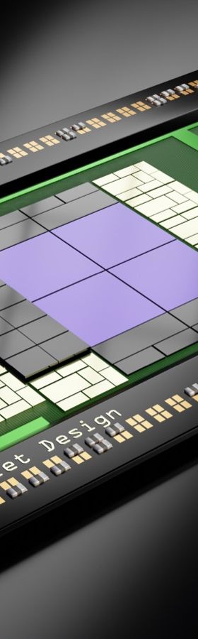
In electronics production, high-precision measurement methods are indispensable if the quality requirements and the performance of components are to be assured continuously. Even the smallest irregularity on the surface of a wafer can jeopardise the entire microchip production process. In other areas of electronics manufacturing as well – in printed circuit board assembly, in the production of optical components and in medical technology – precise 3D inspection is a decisive competitive advantage.
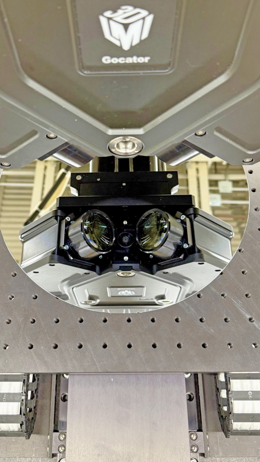
As a partner for high-end metrology, jumavis GmbH knows that genuine precision only becomes possible through the interplay of hardware and sensor technology. For demanding applications the company therefore relies on the precision of the PEAK Metrology positioning system combined with the Gocator 5512 confocal line sensor. This combination makes quality control not only more accurate but also more efficient.
A foundation for the highest precision
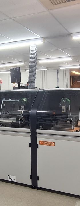
The positioning system from PEAK Metrology allows work to be carried out accurate to the submicrometre, which is what makes repeatable 3D measurement at the relevant inspection points possible in the first place. Environmental influences such as vibration are effectively eliminated, because the massive granite table of the measuring system provides for vibration-free measurement. The complete system solutions are designed to be operated both in production and in the laboratory.
The software and the finely tuned control mechanisms ensure faultless synchronisation with the optical sensor, so that every measurement is carried out under ideal conditions. A decisive advantage for manufacturers in the semiconductor industry is the combination of vibration-free high-precision mechanics and advanced software engineering. X-Y stitching scans several tracks and combines them into a precise overall image, while Z stitching merges different layer heights into a detailed 3D image. Continuous positioning in the submicrometre range ensures that all surface areas can be examined without distortion and that the object always remains in the focus of the confocal line sensor.
A detailed look at surface quality
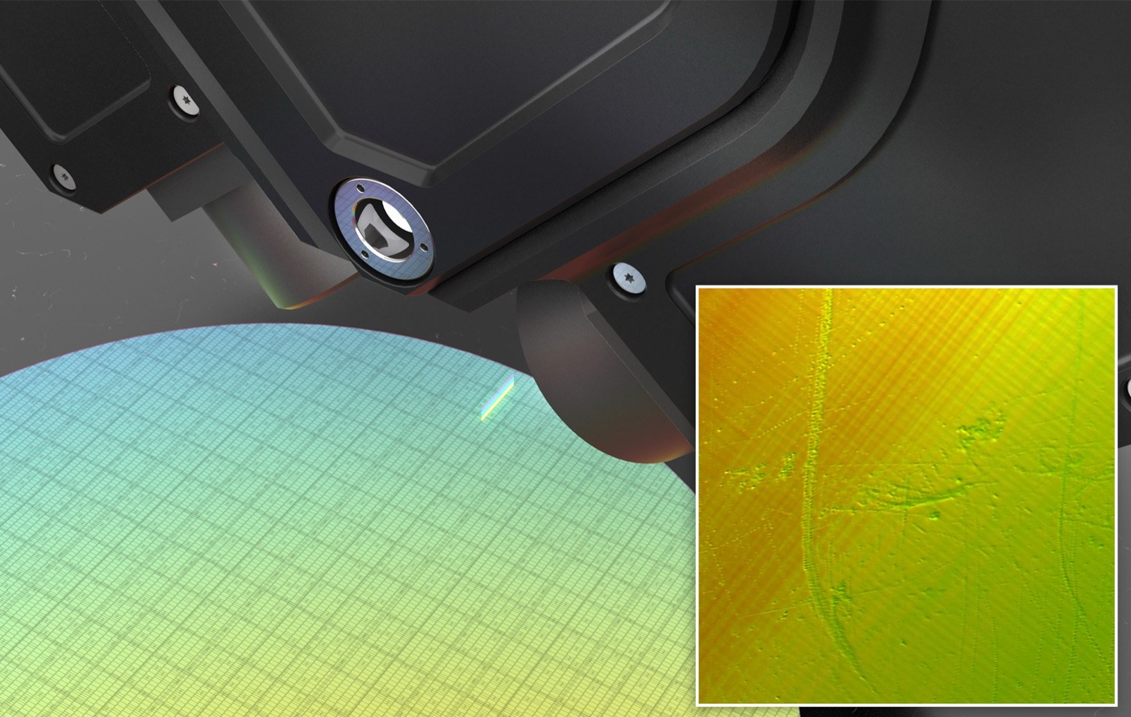
Confocal sensor technology and optical profiling are two of the most advanced technologies for surface analysis in wafer production. These techniques make it possible to produce precise 3D models of surfaces in order to detect defects or irregularities in microscopic dimensions, with a resolution in the nanometre range.
The intelligent sensors of the Gocator 5500 series feature a unique confocal imaging capability using LCI technology. In a single step, the system generates 3D topographies and tomographies as well as 2D intensity data.
LCI (Line Confocal Imaging) uses focused light to produce high-resolution images of surfaces at different depths. This identifies faults in the layers of a wafer that could impair the functionality of the finished microchip.
Optical profiling, by contrast, uses the depth discrimination of focused light waves to reconstruct surfaces in 3D and to represent even the smallest structural anomalies in the micro and nano range that are of great importance for the manufacturing process.
Benefits of combining positioning, confocal line scanning and profiling
- Maximum precision: high-accuracy positioning makes it possible to measure all relevant surface areas precisely and to reproduce them exactly, so that even the tiniest irregularities are detected.
- Avoidance of measurement errors: the positioning system prevents distortion caused by incorrect alignment and thereby minimises sources of error during measurement.
- Optimisation of production quality: continuous monitoring of surface quality leads to higher product quality and reduces scrap.
- Greater efficiency: automated positioning saves time and improves the efficiency of the manufacturing process.
- Versatility: the positioning system can be used not only in wafer production but also in other areas of electronics manufacturing, such as the assembly of printed circuit boards or the production of optical components.
Case examples
In the semiconductor industry it has been shown that precision in wafer production can be increased significantly through the use of such coordinated systems. In practice, surface defects that conventional systems would have overlooked for lack of stability or resolution were detected and remedied at an early stage. The result is a reduced defect rate together with a higher overall yield.
Similar successes have been achieved in general electronics manufacturing. In the assembly of complex printed circuit boards, this complete system solution decisively improved measurement accuracy and eliminated potential sources of error during the mounting of microcircuits. That safeguards the long-term reliability of the end products and protects against costly complaints.
Conclusion
The interplay of the extremely finely controlled mechanics from PEAK Metrology and the sensor technology from LMI Technologies represents a key technology for modern electronics manufacturing. Stable positioning in the submicrometre range forms the necessary foundation for the precise work of the Gocator 5512 confocal line sensor. The economic advantage is the short payback period.
Combining confocal sensor technology and optical 3D profiling raises quality assurance to a new level. Companies gain a tool with which to meet the highest quality standards, reduce scrap sustainably and avoid consequential faults. For the user there is considerable added value, because this complete system solution allows a high degree of flexibility in adapting processes quickly to different product variants. Ultimately this technological edge leads to a significant reduction in overall costs and to greater competitiveness in a demanding market environment. Through its strategic partnerships, jumavis GmbH offers users synergetic know-how for efficient solutions in quality assurance.
Author: jumavis GmbH, Waldbronn, jumavis.de