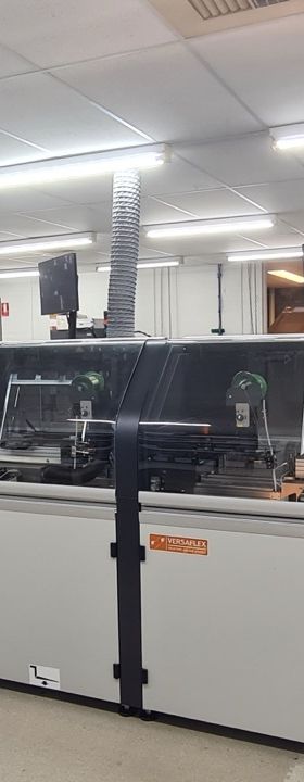
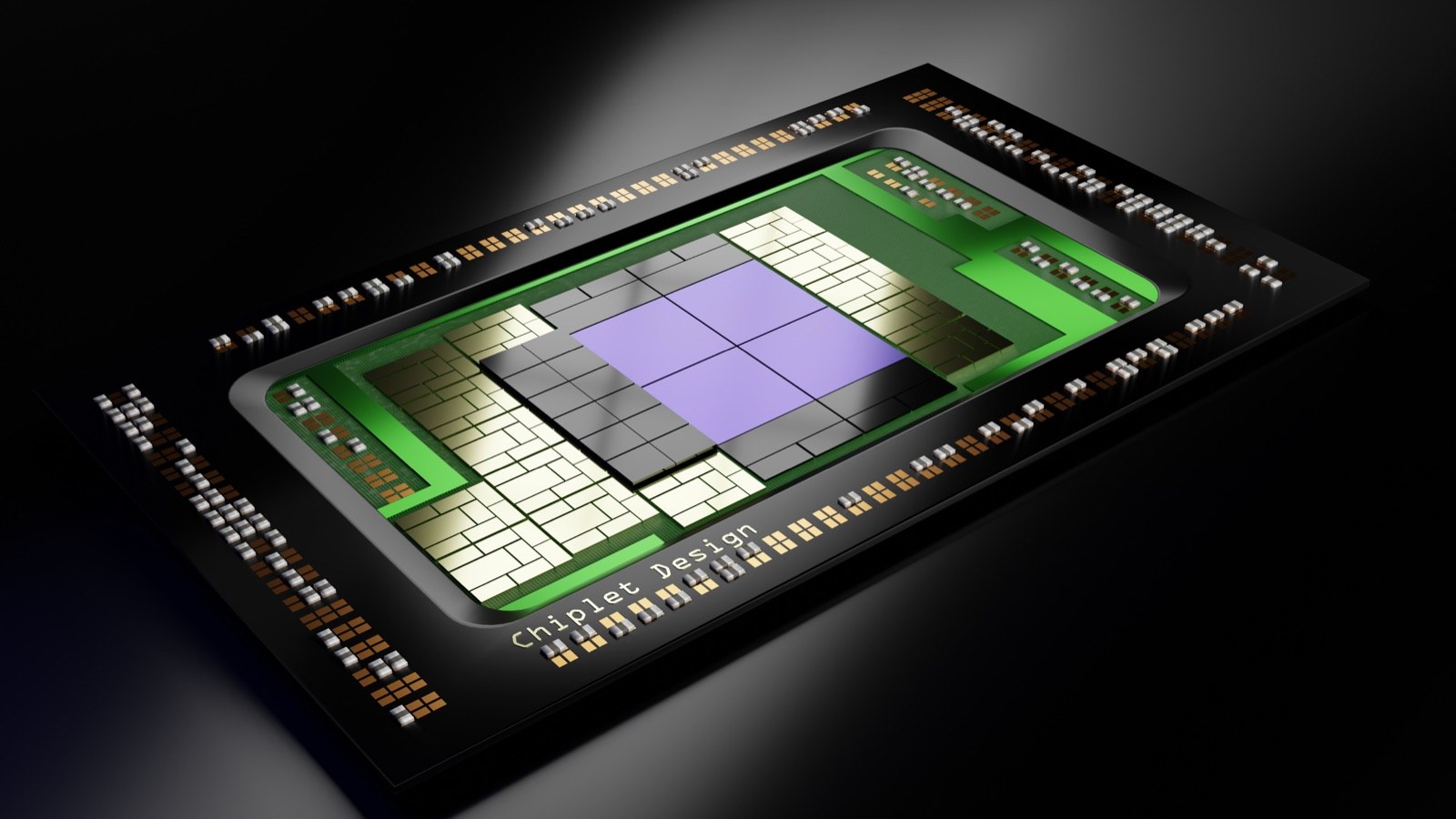
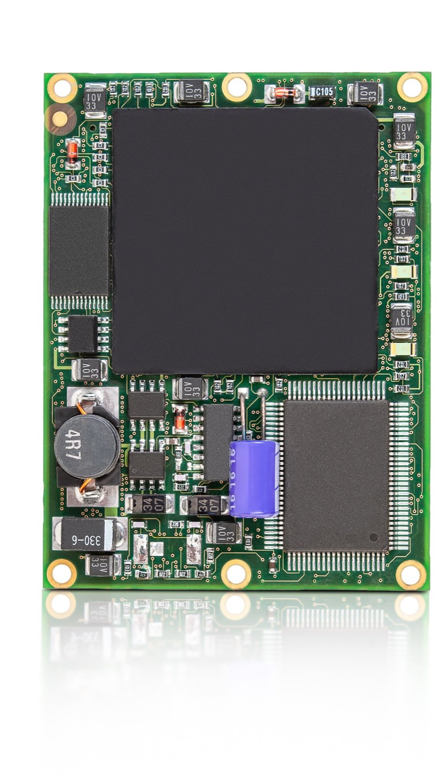
The semiconductor back end, known as packaging, follows the same principle. There, too, a multi-chip construction delivers higher integration, and a modular building-block approach replaces dedicated chip development. Anyone researching the term chiplet will find exactly this concept: modules, and even complete systems, integrated into a single package.
What both solutions share is solderability in the SMT process, because in both cases a complete system is placed in a BGA format. The difference: SoMs are small printed circuit boards, while the package is a self-contained component.
For SoMs, SGeT (Standardization Group for Embedded Technology e.V.) has defined the Open Standard Module [1]. It specifies the module sizes, the interface specifications and the contact grid with its pad sizes and spacings. This allows a developer to become a module designer, or to prepare their own assembly for integrating a module.
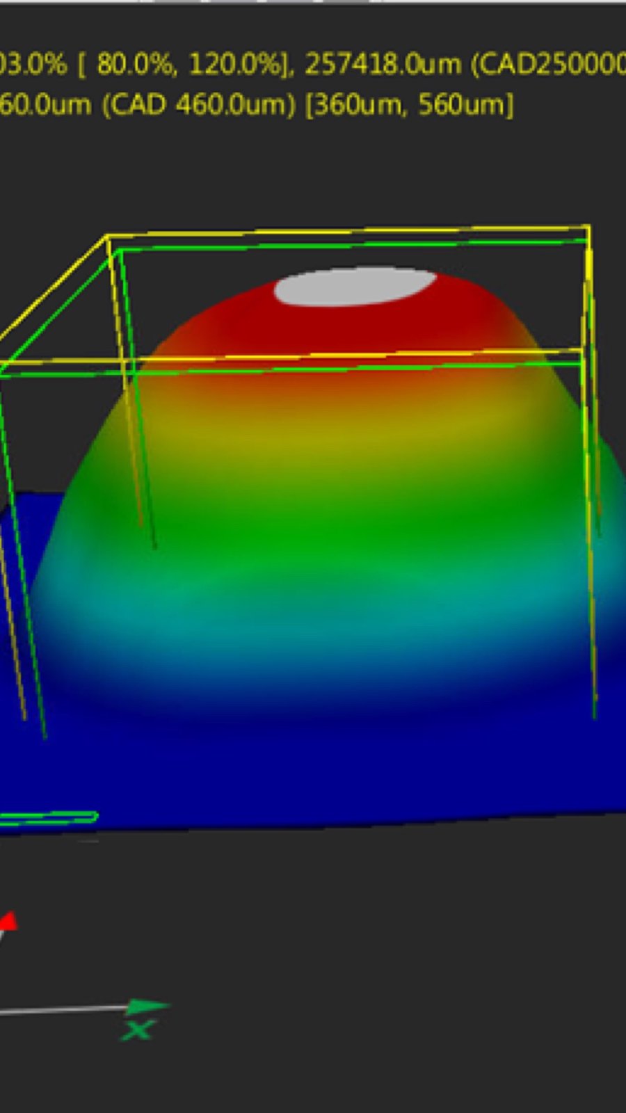
The BGA format is common for System on Modules, though not mandatory. There is also the LGA format, and, for applications with enough space, plug-in cards, which however protrude upwards from the assembly. Anyone who wants to stay small and compact ends up with LGA or BGA. The BGA already brings its own solder depot and is therefore easier to process than the LGA, where the customer has to supply the paste. The OSM specification reflects exactly this: it prescribes a symmetric LGA package and leaves the manufacturer the choice between Fused Tin Grid Array, ENIG LGA and BGA. For measurement these are three different objects: a flat gold-plated area, a domed tin cap and a full solder sphere.
A further parallel between SMT and semiconductor packaging shows up in design. In both cases, a great deal of know-how goes into material selection and thermal management. The critical characteristics are the flatness of the substrate and that of the interconnect bumps. If package or module warps too much, soldering defects such as head-in-pillow occur. The flatter the module or package, the lower this risk during soldering. From this follows the shared inspection task: interconnect bumps and substrate flatness. Two production worlds, one measurement task.
Anyone wanting to check flatness will find dedicated rule sets in both worlds. For the component, JEDEC is responsible: JESD22-B108B describes how to measure the coplanarity of the terminals at room temperature, JESD22-B112 the warpage of the package at reflow temperature. For the printed circuit board, IPC-9641, the “High Temperature Printed Board Flatness Guideline”, records warpage across the entire reflow profile, and explicitly as a local value at the BGA land patterns rather than globally across the board. The bridge between the two is IPC-7095E, which recommends qualifying components for warpage to JESD22-B112, with exactly the reasoning given above: packages that warp too much are prone to head-in-pillow. Concrete figures come from JEITA ED-7306, which sets the maximum permissible warpage for BGA and FBGA at 0.10 to 0.25 mm depending on ball pitch, as an absolute value rather than a percentage of component size. Of that, 80 % is allocated to the package and 20 % is reserved for the warpage of the board. Because the limit itself does not scale, a large module has to be relatively flatter across its diagonal than a small one.
A System on Module is a printed circuit board used as a component, and therefore falls precisely into the seam between these rule sets. The OSM standard itself names no value for flatness. That is an argument for measuring planarity in your own production rather than relying on a specification that does not exist for this format.
In principle, the demands on the measurement system are identical; the differences lie in the surrounding conditions. The packaging process usually takes place in a higher cleanroom class than SMT manufacturing. Modified SMT machines are therefore a common sight in the classic semiconductor back end. Another difference is bump size. A System on Module uses a comfortable 1.25 mm grid with 0.8 mm pads on the substrate side, while µBGA interconnects are inspected in the classic back end. In wafer-level packaging the range extends all the way down to 30 µm bumps.
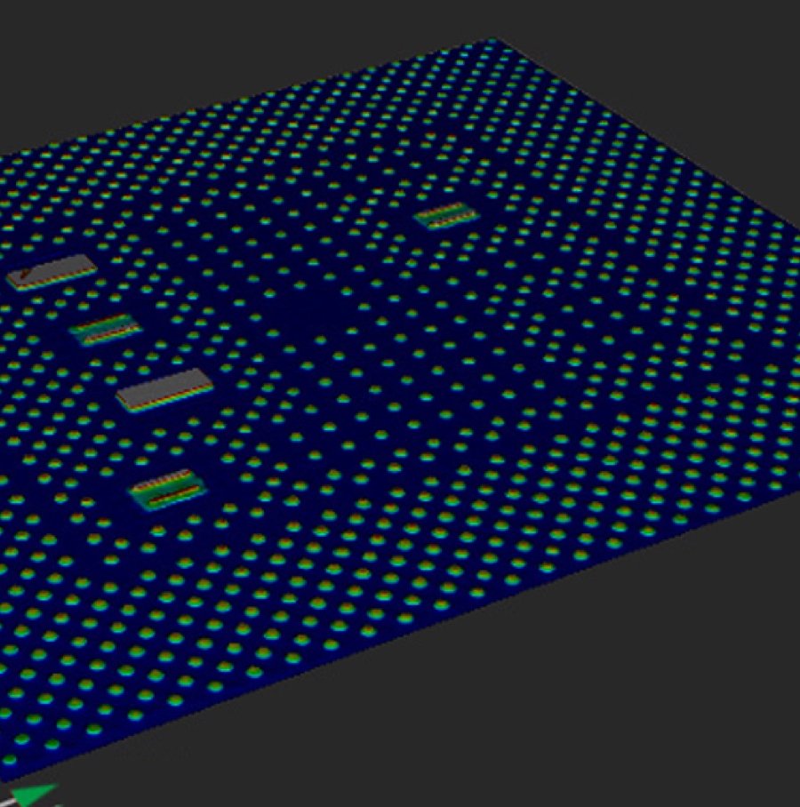
With the development of advanced wafer-level packaging, those modified SMT machines turned into tailor-made hybrid solutions for inspection directly at wafer level. The measuring principle remained intact at its core, but was developed further and extended to meet the higher demands. At Koh Young this development can be traced along the company’s own product line: the Zenith AOI became the Meister D back-end solution, and the Meister D became the ZenStar wafer-level packaging platform, wafer handler included. For SPI, the aSPIre 3 became a Meister S, and the Meister D became the ZenStar as well.
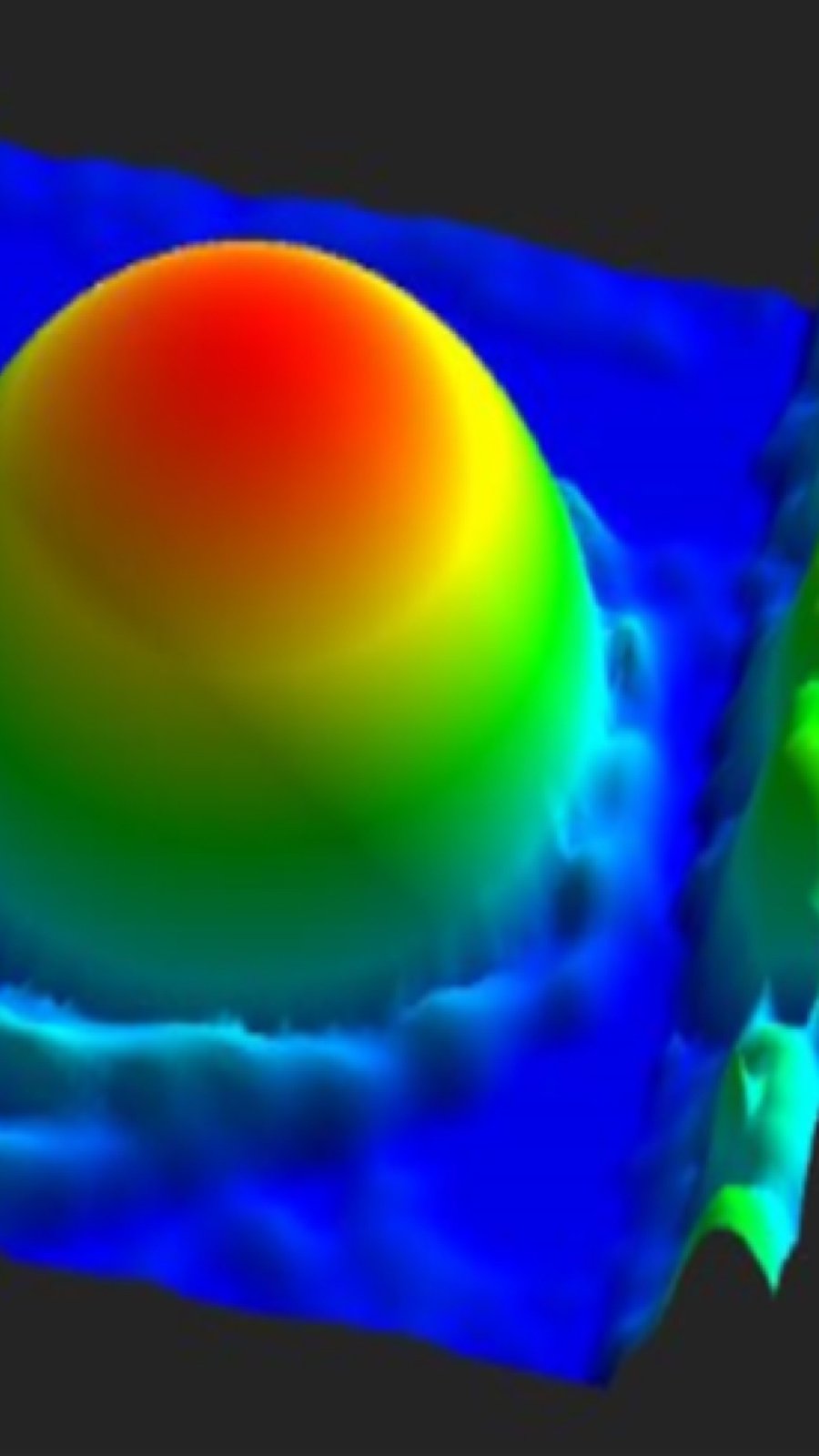
“Evolution” is probably the wrong word for this, because the synergies work in both directions. The semiconductor side contributes expertise in selecting materials and making them work together, in stabilising processes and in maximising yield. SMT brings the knowledge of automation, volume production and cost reduction. It therefore makes sense to try out in one world what works in the other, and to adopt it where it proves itself. The best example is the measurement systems.
Let us stay with the measurement of interconnect bumps. In packaging it was quickly recognised that inspecting balls or bumps does not commit you to an AOI measurement. The reason lies in the measuring principle.
At first glance the AOI looks like the obvious choice, because it can illuminate reflective spheres using many different light channels. An AOI, however, projects its measuring light almost vertically from above so that it can also illuminate and capture the areas between components. To do so it generally uses more measuring channels, but the steep configuration costs accuracy in the Z direction. A typical AOI in the SMT field measures 3D across a range of 4 to 5 mm. Its accuracy is therefore often quoted as a percentage rather than in micrometres. The usual ±3 % refer to the object being measured, not to the measuring range. On a 500 µm ball that comes to ±15 µm, a band of 30 µm. Were the figure tied to the measuring range, an AOI would be useless for such tasks and nobody would buy one. The limit lies elsewhere: the smaller the height to be measured, the less the Z resolution of the AOI suffices to resolve it at all. That is precisely why the SPI exists. The smallest component sizes stand around 120 µm high, solder paste printing works with stencil thicknesses of 60 to 150 µm, and the deposits have to be measured well below that. Calibration adds to this. AOIs are calibrated linearly against several height targets covering the whole measuring range, yet even the smallest of those targets is several hundred micrometres high. An SPI, by contrast, is calibrated against a 100 µm target to ±1 µm. That is where the real difference in accuracy lies.
An SPI works with a flatter projection angle and thereby achieves a very fine resolution in the Z axis of ±1 µm. The decisive factor is the triangulation angle: the steeper the projection, the larger the measuring range and the coarser the Z resolution. The flatter the projection, the finer the z-resolution and the smaller the measuring range. This is why the maximum measuring height of an SPI lies between 400 and 600 µm. Alongside height, reflection plays a role here as well, and it follows from the projection angle. In practice, 300 µm has proven to be the safe range. Above 400 µm, noise and interference from reflections increase, producing out-of-range errors, in other words gaps in the 3D reconstruction.
There is no sharp boundary here, because the working ranges overlap. An AOI measures small components down to around 120 µm in height, provided its resolution is set up for it, for instance to a 10 µm pixel size. That also brings smaller ball heights within reach, and down to roughly 300 µm the AOI still works reliably. Below that it gets tight, because as balls shrink so do the requirements for planarity and height tolerance. JEITA ED-7306 stages the permissible warpage in exactly this way, by ball pitch, from 0.25 down to 0.10 mm, and at some point the Z resolution of the AOI can no longer represent that requirement. The SPI comes from the other side and, for the optical reasons given above, ends at around 300 to 350 µm. Between roughly 300 and 400 µm, therefore, both methods work and the choice depends on the application. Above that it is an AOI task, below it one for the SPI. In packaging, bumps are inspected almost exclusively with SPI-based measurement systems; in SMT, with AOIs. That may change as modules become smaller or as a higher I/O count calls for a finer pitch. Whichever method is used, SPI and AOI alike always capture the entire camera field, and with it the warpage of the substrate as well as the bump height.
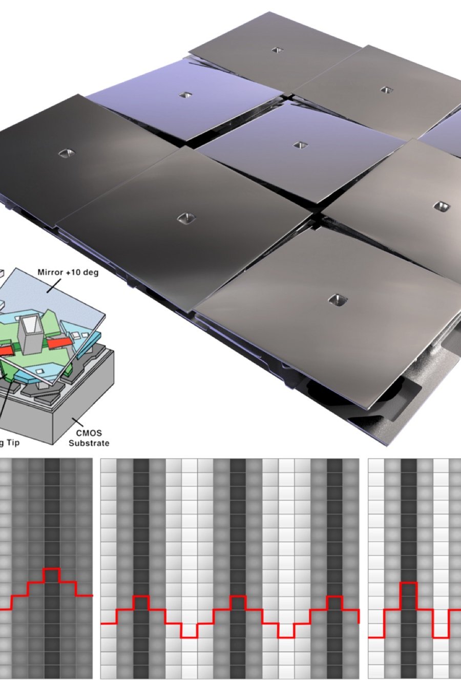
There are also measurement systems on the market that offer a flexible measuring height and are meant to cover both the AOI and the SPI range. They generate the moiré fringes digitally, so the fringe pitch can be programmed freely. That sounds good at first, but in practice the same physical principles apply: at large measuring heights you become just as inaccurate. On top of that, the digital projector is itself resolved into pixels, or more precisely into small mirrors. You are therefore tied to a fixed grid. An analogue system divides the transition from white to black into 256 shades of grey. With a digital projector, very fine fringes leave only a few mirrors between two lines. Yet it is precisely the fine gradation of grey values that determines accuracy. The supposed flexibility is bought at the price of accuracy.
In Europe this meets the classic “all in one” problem. Production floor space and investment budgets are limited, so people look for a machine that can do everything. A Swiss army knife can cut, drive screws, open bottles, saw and pull corks. And yet at home we still keep a toolbox, several pairs of scissors and a waiter’s corkscrew. Why? Because multifunctionality is no substitute for precision!
Here SMT can learn from packaging, because there the message has arrived. Components are inspected with AOIs, bumps with the more accurate SPIs. Multifunctionality plays no part.
That pitches keep shrinking is no guess. The Heterogeneous Integration Roadmap published by the IEEE Electronics Packaging Society puts the minimum solder ball pitch across all wafer-level formats at 200 µm up to 2021, 175 µm up to 2023 and 150 µm from 2024 onwards [2]. For SMT this means what it has experienced all along: once the component industry builds smaller, manufacturing follows. Larger formats are eventually discontinued for cost reasons, and SMT is obliged to follow the trends set by packaging and semiconductor, whether it wants to or not. Among passive components, this very mechanism has driven production towards ever smaller component sizes over the years.
For the future, clear developments are emerging in both worlds. In SMT, modular systems are becoming ever more complex and finer in pitch. In the packaging industry, applications continue to shift towards wafer level in order to cut cost and effort there as well. In both cases the accuracy requirements rise, and that calls for users to be open towards SPI for smaller bump sizes. In the packaging industry this is long since the case. In SMT it still takes some persuasion, and the insight that the requirements determine the measurement system, not the wish for flexibility.
Links
- [1] SGeT: Open Standard Module (OSM) Hardware Specification V1.2, sget.org/standards/osm
- [2] IEEE Electronics Packaging Society: Heterogeneous Integration Roadmap, 2021 Edition, Chapter 23: Wafer-Level Packaging (WLP), Table 4, eps.ieee.org — all chapters at eps.ieee.org/hir