
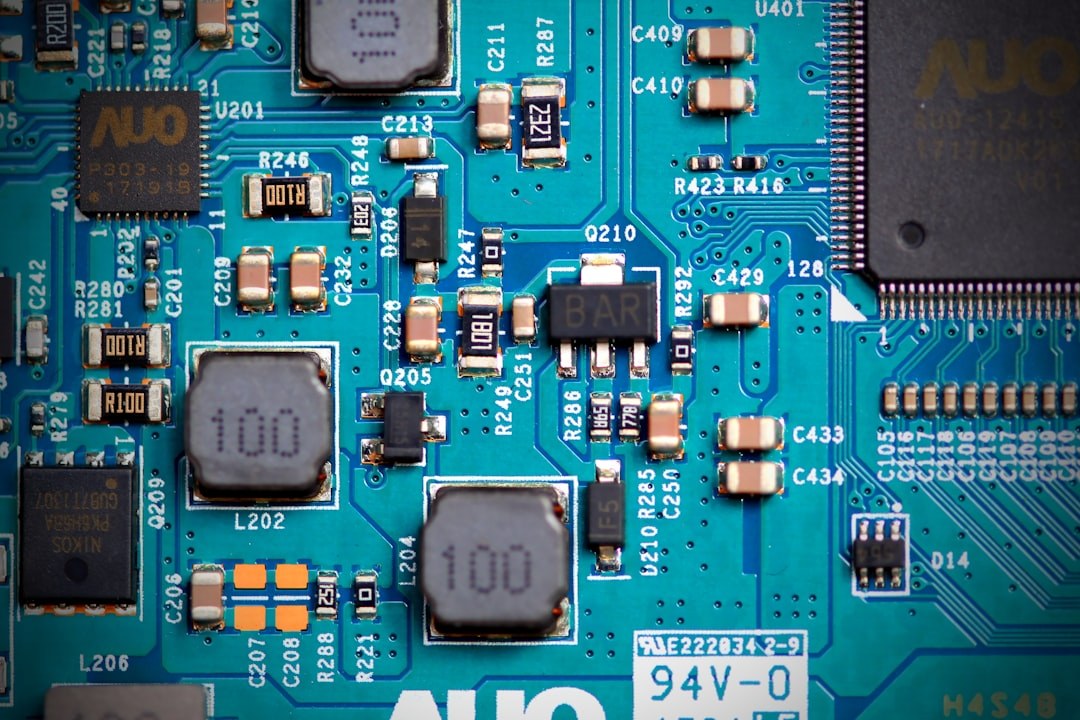
In surface-mount technology, stencil printing is the first and arguably most consequential process step in the entire assembly chain. Before any component is placed, before reflow ovens reach their peak temperatures, the quality of every solder joint is largely predetermined by the volume, shape and position of the solder paste deposit. Industry analyses consistently attribute between 60 and 70 percent of all SMT soldering defects — including bridging, insufficient solder, tombstoning and open joints — to errors introduced at the printing stage. This makes a thorough grasp of stencil printing fundamentals not a theoretical luxury but a practical necessity.
The stencil printing process appears deceptively simple: a metal stencil is aligned over a bare PCB, solder paste is applied, and a squeegee blade traverses the stencil surface, forcing paste through the apertures onto the underlying pads. In practice, however, the process involves a complex interaction of material properties, mechanical parameters and environmental conditions, each of which must be understood and controlled to achieve consistent, defect-free deposits.
Stencil design and aperture geometry
The stencil itself is typically laser-cut from stainless steel foil with thicknesses ranging from 100 µm to 150 µm for standard SMT work, and down to 80 µm or below for fine-pitch and miniaturised components. The aperture geometry — its size, shape and wall finish — directly determines how much paste is deposited and how cleanly it releases from the stencil.
A key design metric is the area ratio (AR), defined as the aperture opening area divided by the aperture wall area. Industry experience has established that an area ratio of 0.66 or higher is required for reliable paste release. Below this threshold, surface tension between the paste and the aperture walls exceeds the force available to push the paste onto the pad, resulting in insufficient deposits and inconsistent transfer efficiency. For very small apertures serving components such as 0201 or 01005 chip resistors, achieving adequate area ratios often necessitates step stencils — localised thinned or thickened zones — or electroformed nickel stencils, which offer smoother wall surfaces and improved release characteristics.
Aperture walls are routinely treated with nano-coatings or electropolished after laser cutting to reduce roughness and minimise paste adhesion to the walls. The trapezoidal aperture — slightly wider at the board side than the squeegee side — further assists paste ejection by reducing mechanical resistance during release.
Solder paste properties and their process implications
Solder paste is a suspension of metal alloy powder in a flux medium. The powder particle size, specified in IPC Type designations (Type 3 through Type 7 and beyond), must be matched to the smallest aperture dimension on the board. The commonly applied guideline recommends that the aperture width be at least five times the maximum particle diameter of the paste, ensuring unobstructed flow through the aperture and preventing particle bridging or clogging.
Rheologically, solder paste behaves as a thixotropic material: its viscosity decreases under shear — as applied by the moving squeegee — and recovers when the shear stress is removed. This behaviour is what allows the paste to flow through apertures during printing and then hold its shape on the pad immediately afterwards. Temperature significantly affects viscosity, which is why most process specifications require paste and PCBs to be equilibrated to a stable room temperature — typically between 23 °C and 25 °C — before printing commences.
The transition from tin-lead (SnPb) to lead-free alloys, primarily SAC305 (Sn96.5/Ag3.0/Cu0.5), has also affected paste printing behaviour. Lead-free pastes generally exhibit higher viscosity and different slump characteristics, requiring tighter process control, particularly with regard to aperture design and squeegee parameters.
Key process parameters: squeegee speed, pressure and separation
Three mechanical parameters dominate printing quality: squeegee speed, squeegee pressure and stencil separation speed. The squeegee, usually a hardened polyurethane or metal blade, must roll paste ahead of itself to fill apertures through a hydrodynamic wedge effect. If speed is too high, the paste does not have sufficient time to flow into small apertures; if too low, the paste may smear or exhibit excessive slump.
Squeegee pressure — measured in Newtons per linear millimetre of blade length — must be sufficient to wipe the stencil surface clean without excavating paste from already-filled apertures. Excessive pressure accelerates stencil wear and forces paste under the stencil, causing smearing and bridging. Insufficient pressure leaves residual paste on the surface, increasing the risk of shorts between adjacent pads.
Stencil separation — the controlled vertical lifting of the stencil away from the board after printing — is a critical yet often underestimated parameter. A slow, controlled separation allows paste to release cleanly from the aperture walls by giving surface tension time to act in favour of adhesion to the pad rather than the stencil wall. Separation speeds between 0.5 mm/s and 3 mm/s are common, with finer pitch assemblies requiring the lower end of this range.
Solder paste inspection and process feedback
Modern SMT lines universally integrate automated solder paste inspection (SPI) systems immediately after the printer. These systems use structured light, laser triangulation or fringe projection to measure the three-dimensional volume, height, area and offset of every paste deposit on the board. SPI is not merely a quality gate; when connected to the printer via closed-loop feedback, it enables real-time correction of systematic drift — caused by paste drying, temperature changes or gradual stencil wear — before defective boards are produced.
IPC-7525 provides the industry standard for stencil design guidelines, while IPC-A-610 defines acceptability criteria for the finished assembly. Together, these documents give engineers a normative framework for both upstream design decisions and downstream quality assessment. Data from SPI systems, when stored and analysed over time, also forms the basis for statistical process control and feeds into broader traceability and MES architectures in smart factory environments.
Practical guidance and outlook
For production engineers, the most effective approach to stencil printing optimisation begins with a structured design-of-experiment (DoE) methodology, systematically varying one parameter at a time — squeegee speed, pressure, separation speed, underside cleaning frequency — while monitoring SPI output metrics. Underside stencil cleaning, typically performed every 5 to 20 print cycles depending on paste type and aperture density, prevents paste accumulation beneath the stencil from causing smearing and satellite deposits.
As component miniaturisation continues to push towards Type 6 and Type 7 paste powders and area ratios that challenge even nano-coated electroformed stencils, the physics of paste release and aperture fill become ever more demanding. Emerging approaches such as jet printing — dispensing paste without a stencil through piezoelectric nozzles — offer an alternative path for ultra-fine-pitch and mixed-technology boards, though stencil printing remains the dominant and most cost-effective method for high-volume SMT production. Mastering its fundamentals is therefore an enduring requirement for anyone responsible for SMT process quality.