Zum Inhalt springen
EPP Europe
  • News
  • Products
  • Applications
  • Technology
  • Semiconductor
  • Inspection
  • Company News
  • Events
EPP Europe
  • Technology
  • Inspection (AOI/AXI)
  • Semiconductor Packaging
  • Company News
  • Products
  • Trade Shows & Events
    EPP Europe Newsletter
    The most important electronics-manufacturing news delivered to your inbox.

    Info

    • Impressum
    • Datenschutz
    • Barrierefreiheit
    • Datenschutzeinstellungen

    Kontakt zur Redaktion

    EPP EuropeKonradin Mediengruppe
    Ernst-Mey-Str. 8, 70771 Leinfelden-Echterdingen

    E-Mail: redaktion@konradin.de
    Folgen Sie uns
    EPP Europe
    © 2026 EPP Europe
    Startseite/Top-news/Artikel
    Sigma bonder for large die on wafer level substrates
    Foto: Louis Reed / Unsplash
    Top-news

    Sigma bonder for large die on wafer level substrates

    Finetech introduces the new Fineplacer Sigma bonder, designed to provide a solution for large die up to 100 mm, combined with a working area of
    Veröffentlicht
    15. Juli 2016
    Lesezeit
    1 Minute
    Rubrik
    Top-news

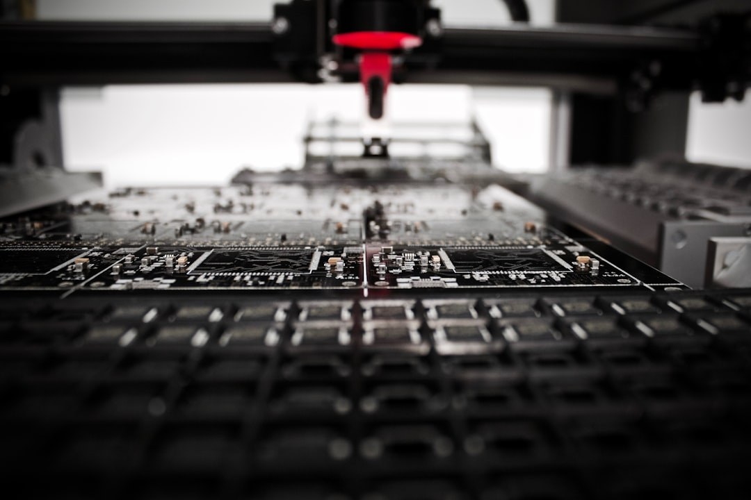
    The system is the ideal choice for a wide variety of Wafer Level Packaging (FOWLP, W2W, C2W) with high bump count used to assemble MEMS/MOEMS, IR/ image sensors, focal plane arrays, and high power device packaging. This includes assembly of complex 2.5D and 3D IC packages that require high accuracy across the entire surface of large substrates. The bonder can also pick up from and bond to 300 mm wafers.

    The cornerstone element of the new bonder is FPXvision, the newest generation of the company‘s Vision Alignment Systems (VAS). It provides the highest resolution at all magnification levels and real-time optimized camera images. It enables the smallest devices and features to be clearly observed across the entire field of view, even with large components and substrates. Touch screen magnifiers allow zoomed images anywhere in the field of view. Two high definition cameras and specially developed optics ensure that the cameras’ full resolution potential is tapped. FPXvision is the first vision system to introduce pattern recognition to a semi-automated die bonding platform.

    The bonder allows endless fields of application to users working with medical technologies, RD, mil/aero, semiconductor, and automotive industries. The optimal process environment can be configured for each type of application, including the latest technologies such as vacuum bonding, sintering or metal diffusion (Cu/Cu).

    www.finetechusa.com

    Mehr aus Top-news

    Weitere aktuelle Artikel aus der Rubrik Top-news.

    Alle Top-news-Artikel
    Indium Corporation and SMT Thermal Technologies to Present Low-Temperature Reflow Energy Savings at EFX 2026Foto: Indium Corporation
    Top-news

    Indium Corporation and SMT Thermal Technologies to Present Low-Temperature Reflow Energy Savings at EFX 2026

    7. Oktober 2026

    Indium Corporation and SMT Thermal Discoveries will jointly demonstrate how pairing Durafuse LT mixed-powder alloy with the SMT R320 convection reflow oven cuts energy costs and emissions by 25% compared with…

    ITW EAE Electrovert EcoWave Wins 2026 NPI AwardFoto: Bermix Studio / Unsplash
    Top-news

    ITW EAE Electrovert EcoWave Wins 2026 NPI Award

    1. Oktober 2026

    ITW EAE has received a 2026 New Product Introduction Award for the Electrovert EcoWave, an option for its wave soldering machine platform.

    Omron Promotes End-to-End Barcode Reading and Sensing for Production TraceabilityFoto: Edgar Cornejo / Unsplash
    Top-news

    Omron Promotes End-to-End Barcode Reading and Sensing for Production Traceability

    8. September 2026

    Omron Inspection outlines an end-to-end barcode reading and sensing approach designed to provide full visibility across electronics production processes, supporting traceability requirements in smart factory…

    Cybord Launches Air-Gapped Visual AI Platform for On-Premises Component Inspection and TraceabilityFoto: Cybord
    Top-news

    Cybord Launches Air-Gapped Visual AI Platform for On-Premises Component Inspection and Traceability

    6. September 2026

    Cybord has announced a fully air-gapped version of its Visual AI component analytics platform, enabling organisations operating restricted or closed networks to run advanced inspection and traceability capabilities…

    ← Zurück zu Top-newsZur Startseite