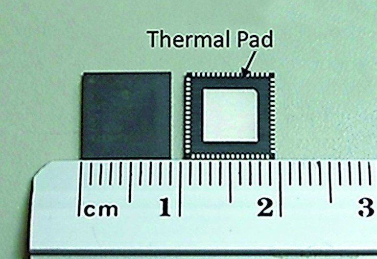
One area of great concern that can impact performance is the fact that BTCs generate a considerable amount of heat during their normal operation. The thermal pad, which is soldered to the receiving pad on the printed wiring board (PWB), is designed to remove this heat. Unfortunately, voids that form during reflow soldering can inhibit this process, causing the BTC to overheat and potentially impact reliability. An informal survey of engineers suggests that this voiding issue is the greatest concern in electronics assembly today.
Why do voids form?
Voids form due to the evaporation of flux materials in the solder paste. Solder paste is about 50 % of volume flux so the amount of these evolved volatile materials during reflow can be considerable.
There is no standard as to how much voiding is acceptable, but there appears to be an agreement that a total void area of less than 50 %, with no “lake” void greater than 40 % of the area, is an absolute requirement; however, 25 % is preferred. In some critical applications such as automotive, 10 % or less is required.
Reducing voiding: past work
To minimize voiding in the past, process engineers had to perform designed experiments to optimize many of the assembly variables, such as reflow profiles and stencil design. Considerable work was done to investigate the effect of stencil designs to create paths for the evolved flux vapors to escape.1) Other work showed the benefit of using solder preforms to maximize the amount of solder between the BTC and the PWB pads.2)
Reducing voiding: current work with reflow ovens
Considerable developments have occurred in reflow oven technology to minimize voiding – most noteworthy has been the use of vacuum reflow to aid in removing voids.3) Reports suggest that these ovens have been successful in reducing voiding to less than a few percent. While this achievement is significant, it requires the assembler to purchase a new oven or at least an upgrade. There have also been anecdotal reports of solder paste spattering, but we expect that process optimization procedures can minimize this problem.
Reflow ovens employing ultrasonic energy have been reported to achieve similar success.4) As Heller Industries stated in a 2016 presentation, “Ultrasonics are applied when solder is in liquid state.” Ultrasonics create cavitation, which stretches voids/bubbles so they combine with other voids, and move to the outer surface of solder to escape. As with vacuum reflow ovens, the process engineer must purchase a new oven or an upgrade.
Reducing voiding: current work with solder paste and process
Recently, Indium Corporation conducted research to determine critical variables in minimizing voids, especially in light of modern solder pastes that have been designed to reduce voiding.5) After considering the many possible variables, they settled upon an experimental plan using the following:
- Entek Plus CU-106A-HT OSP PWB pad finish
- Laser cut, non-nano-coated steel stencils of 100 µm and 125 µm thicknesses
- A windowpane stencil design in the PWB thermal pad area to allow volatiles to escape. The windowpane squares were 0.088 “ on each side
- Squeegee printing speed of 100 mm/s with a pressure of 6 kg
- Printer separation speed of 5 mm/s at a distance of 2 mm
- A stencil wipe (W/D/V) was performed before each board
The QFN they assembled had a square ground plane of 7.75 mm (0.30 “) on a side. They performed reflow in air with Profile #1—a straight ramp profile (0.9 ˚C/second ± 0.1 ˚C/second) and a peak temperature of 241 ˚C ± 4 ˚C for most investigations. However, a second optimized profile (Profile #2) was also investigated to determine the effect of the reflow profile on voiding. A variety of solder pastes was used that had halogen-free and halogen-containing fluxes and different solder particles sizes (e.g., Type 3, Type 4, Type 4.5, and Type 5).
The results were encouraging. Profile #2 (termed the ‘Void reducing optimized profile’) significantly reduced voiding from 22 % to 8 %, as compared to Profile #1. In addition, the standard deviation of the data was much “tighter” for Profile #2. The 125 µm stencil reduced voiding about 4.5 % as compared to a 100 µm stencil. The difference likely being that the 125 µm stencil provided a slightly better standoff to vent the vapors. Regarding solder paste particle size, the company found that only Type 3 solder powder produced statistically significantly different results as compared to Types 4, 4.5, and 5. The Type 3 solder paste produced about 15 % more voiding.
A final experiment was performed in which the effect of different solder paste flux vehicles on voiding was evaluated. Three PCBs, with 12 QFNs each, were used for each solder paste, for a total of 36 QFNs per paste. The results were striking. Some pastes produced only about 5 % voids, while others produced as much as 45 %.
These results were not only surprising, but also very encouraging. solder pastes have now been developed that essentially eliminate voiding.
productronica, Booth A4.214
This was created in a collaboration, with:
Chris Nash, Product Manager PCB Assembly Materials, Indium Corporation
Ron Lasky, PhD, PE, Senior Technologist, Professor of Engineering/Director of the Cook Engineering Design Center, Dartmouth College, and
Andreas Karch, Regional Technical Manager – Germany, Austria and Switzerland, Indium Corporation
References
- N.C. Lee et al. http://www.indium.com/technical-documents/whitepaper/voiding-control-for-qfn-assembly
- Homer, S., Lasky. R, Minimizing Voiding In QFN Packages Using Solder Preforms, SMTAI 2011, Fort Worth, TX.
- http://www.circuitnet.com/news/uploads/2/SMT_Vacuum_void_reduction_Sept2012.pdf
- http://www.hellerindustries.com/Inline-Vacuum-Reflow-System.pdf
- The work is discussed in detail in our paper Minimizing Voiding In SMT Assembly Of BTCs, SMTAI 2016, Chicago, IL.
Zusammenfassung Résumé Резюме
Der Artikel zeigt neue Verfahren bei Low-Standoff-Bauteile während dem Reflowlöten zur Reduzierung von Voiding auf. Dazu wurden Untersuchungen zur Bestimmung der kritischen Variablen für die Minimierung von Voids durchgeführt. Die Ergebnisse waren nicht nur verblüffend sondern auch anspornend. Denn nun sind Lotpasten verfügbar, die Voiding deutlich minimieren.
L’article présente de nouvelles procédures pour les éléments de bas niveau lors du soudage par refusion pour réduire des soufflures. À cette fin, des recherches ont été menées pour déterminer les variables critiques pour la minimisation de soufflures. Les résultats n’étaient pas seulement surprenants mais aussi inspirants. Pour le moment, les pâtes à souder aident à réduire considérablement des formations de soufflures.
В статье рассматриваются новые методы, применяемые при пайке оплавлением компонентов с малым зазором между корпусом микросхемы и печатной платой (stand-off) с целью уменьшения образования пустот. Для этого были проведены исследования, целью которых было определение критических переменных процесса минимизации пустот. Результаты превзошли все ожидания и подстегнули интерес к дальнейшим исследованиям. Теперь доступны паяльные пасты, значительно снижающие образование пустот.