Zum Inhalt springen
EPP Europe
  • News
  • Products
  • Applications
  • Technology
  • Semiconductor
  • Inspection
  • Company News
  • Events
EPP Europe
  • Technology
  • Inspection (AOI/AXI)
  • Semiconductor Packaging
  • Company News
  • Products
  • Trade Shows & Events
    EPP Europe Newsletter
    The most important electronics-manufacturing news delivered to your inbox.

    Info

    • Impressum
    • Datenschutz
    • Barrierefreiheit
    • Datenschutzeinstellungen

    Kontakt zur Redaktion

    EPP EuropeKonradin Mediengruppe
    Ernst-Mey-Str. 8, 70771 Leinfelden-Echterdingen

    E-Mail: redaktion@konradin.de
    Folgen Sie uns
    EPP Europe
    © 2026 EPP Europe
    Startseite/Top-news/Artikel
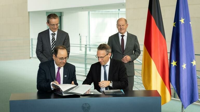
    Intel, German Government agree on increased subsidies for wafer fab in Magdeburg
    Bildquelle nicht angegeben
    Top-news

    Intel, German Government agree on increased subsidies for wafer fab in Magdeburg

    US semiconductor giant Intel and the German federal government have reached an agreement to increase state subsidies for the company’s planned wafer
    Veröffentlicht
    20. Juni 2023
    Lesezeit
    3 Minuten
    Rubrik
    Top-news

    Intel says the change reflects the expanded scope and change in economic conditions since the site was first announced.

    The company plans to construct two leading-edge semiconductor facilities (also known as “fabs”) in Germany. The first facility is expected to enter production in four to five years following the European Commission’s approval of the incentive package. Given the current timeline and scale of the investment, the company plans to deploy more advanced Angstrom-era technology in the facilities than originally envisioned. The Magdeburg site will serve Intel products and Intel Foundry Services customers.

    The site is expected to create 7,000 construction jobs over the course of the first phase of the build, approximately 3,000 permanent high-tech jobs at Intel and tens of thousands of additional jobs across the industry ecosystem.

    “Building the ‘Silicon Junction’ in Magdeburg is a critical part of our strategy for Intel’s growth. Combined with last week’s announcement of our investment in Wrocław, Poland, and the Ireland sites we already operate at scale, this creates a capacity corridor from wafers to complete packaged products that is unrivaled and a major step toward a balanced and resilient supply chain for Europe,” said Intel CEO Pat Gelsinger. “We’re grateful to the German federal government, Chancellor Olaf Scholz and the government of Saxony-Anhalt for their partnership and shared commitment to fulfilling the vision of a vibrant, sustainable, leading-edge semiconductor industry in Germany and the EU.“

    Chancellor Olaf Scholz of Germany said, “Today’s agreement is an important step for Germany as a high-tech production location – and for our resilience. Intel‘s semiconductor production in Magdeburg is the single largest foreign direct investment in German history. With this investment, we are catching up technologically with the world’s best and expanding our own capacities for the ecosystem development and production of microchips. This is good news for Magdeburg, for Germany and for all of Europe.”

    Vice Chancellor and Federal Minister for Economic Affairs and Climate Action Robert Habeck said, “Today‘s agreement is a milestone for Germany as a location for innovation and investment, for jobs, resilience and competitiveness. Intel‘s investment will raise semiconductor production in Germany to a new level and is an important contribution to growing European sovereignty.”

    Intel says its investment will drive significant economic benefits not only in Magdeburg and Saxony-Anhalt, but across the country and throughout the European Union. „The new wafer fabrication site in Magdeburg will create a first-of-its-kind, leading-edge end-to-end semiconductor manufacturing value chain in Europe, serving European customers and helping to fulfill the EU’s ambitions for a more resilient semiconductor supply chain,“ the company said.
    Mehr aus Top-news

    Weitere aktuelle Artikel aus der Rubrik Top-news.

    Alle Top-news-Artikel
    Indium Corporation and SMT Thermal Technologies to Present Low-Temperature Reflow Energy Savings at EFX 2026Foto: Indium Corporation
    Top-news

    Indium Corporation and SMT Thermal Technologies to Present Low-Temperature Reflow Energy Savings at EFX 2026

    7. Oktober 2026

    Indium Corporation and SMT Thermal Discoveries will jointly demonstrate how pairing Durafuse LT mixed-powder alloy with the SMT R320 convection reflow oven cuts energy costs and emissions by 25% compared with…

    ITW EAE Electrovert EcoWave Wins 2026 NPI AwardFoto: Bermix Studio / Unsplash
    Top-news

    ITW EAE Electrovert EcoWave Wins 2026 NPI Award

    1. Oktober 2026

    ITW EAE has received a 2026 New Product Introduction Award for the Electrovert EcoWave, an option for its wave soldering machine platform.

    Omron Promotes End-to-End Barcode Reading and Sensing for Production TraceabilityFoto: Edgar Cornejo / Unsplash
    Top-news

    Omron Promotes End-to-End Barcode Reading and Sensing for Production Traceability

    8. September 2026

    Omron Inspection outlines an end-to-end barcode reading and sensing approach designed to provide full visibility across electronics production processes, supporting traceability requirements in smart factory…

    Cybord Launches Air-Gapped Visual AI Platform for On-Premises Component Inspection and TraceabilityFoto: Cybord
    Top-news

    Cybord Launches Air-Gapped Visual AI Platform for On-Premises Component Inspection and Traceability

    6. September 2026

    Cybord has announced a fully air-gapped version of its Visual AI component analytics platform, enabling organisations operating restricted or closed networks to run advanced inspection and traceability capabilities…

    ← Zurück zu Top-newsZur Startseite