The company’s portfolio includes a range of products lines from Optical CMM, laser and 3D scanners, to X-ray and Computed Tomography (CT) inspection systems, vision systems, microscopes and optical inspection systems.
This range of products is used throughout the world, in a variety of different industries, backed by a customer service which includes in-house specialists. With offices located across Europe, Nikon Metrology works on the principle of being a market-leader in its field by providing innovative state-of-the-art products, underpinned by a complete after-sales service.
Today there is a growing demand for flexible, high-resolution and cost-effective inspection systems to cope with the demands of ever-smaller electrical components and comply with tighter quality standards. Specialists in Tring, develop and manufacture X-ray systems and CT inspection systems that get the inside picture of complex industrial and electrical parts, by looking into the internal structure. The CT capability is used to qualify and quantify any inner or outer dimension in a smooth, non-destructive process. X-ray electronics inspection systems respond to a growing demand for flexible, detailed and affordable inspection to cope with the demands of ever-smaller electrical components and comply with tighter quality standards.
One area where Nikon Metrology is pushing boundaries, is through its work on providing products for small devices. The most challenging aspect for electronics inspection at the moment is the persistent demand for miniaturisation with technological advances for example, 3D stack devices, fully integrated with processors, memory as well as sensors such as MEMs. The challenge comes from how to clearly identify the smallest, finest defects, with 100% confidence every time.
The drive for higher performance, lower power consumption and higher capacity is resulting in smaller and smaller devices, in terms of packaging technology, denser and smaller interconnect technologies, which also result in increased multi-stacked packages. These multi-tiered packages are challenging traditional X-ray inspection as a lot more features and details are present at any one time during an inspection. The increase in the use of multi-layer boards, has resulted in the need for more experienced operators to efficiently detect defects, which in turn makes inspection times longer.
Nikon Metrology is working on building the next generation systems to detect the smallest defects in order to have the highest throughput capability. One such initiative to answer these challenges is XT V 160NF inspection platform, one of the most recent products to be added to the portfolio. This system provides next generation imaging capability, down to 0.1um feature recognition capabilities, higher speed manipulator with super accurate micron accuracy. Included is a high definition flat panel detector ideal for the smallest interconnects for example TSV and copper pillar which are currently challenging the industry. It also features innovative laminography capabilities, X.Tract, allowing defined CT views of any large PCBA or wafer without requiring the cutting of the board.
X.Tract, that can be also used in standard XT V 160 systems was recently launched at the Electronica show and provides CT-quality inspection of complex multi-layer electronics assemblies without slicing them. The product enables virtual micro-sections in any direction in the desired area of interest. Detecting defects obscured in 2D X-ray images of complex components such as Package on Package (PoP) or double-sided boards. The result is a better insight which in turn reduces false call rates and higher productivity.
Further initiatives from Nikon Metrology include the XT H 225 ST industrial CT inspection system which is ideally suited for dealing with a wide range of materials and sample sizes, especially those that are too large or heavy for other systems in their range. It features a proprietary Nikon Metrology 225 kV micro focus source with reflection target and 3 µm spot size for superior precision and performance. With the optional transmission target, you obtain an even smaller spot size and higher magnification for brilliant, high-contrast images.
Regardless of the target choice, the system uses an open-tube X-ray micro focus source that guarantees a lower cost-of-ownership. The core of the processing power is situated in the XT software suite, which not only optimises the sample throughput, but also simplifies the system operation. A CT wizard guides operators through the data acquisition process and customisable macros automate the measurement workflow. The open X-ray tube allows for user-friendly local maintenance of internal tube components. For a greater versatility the system can be configured with different flat panels or source configurations to provide a system ideally suited to your needs. The system can be equipped with three interchangeable sources; the 225 kV reflection target, the 180 kV transmission target and 225 kV rotating target. Combined with the wide range of flat panel detectors to choose from the system provides a flexible tool for quality laboratories, production facilities and research departments.
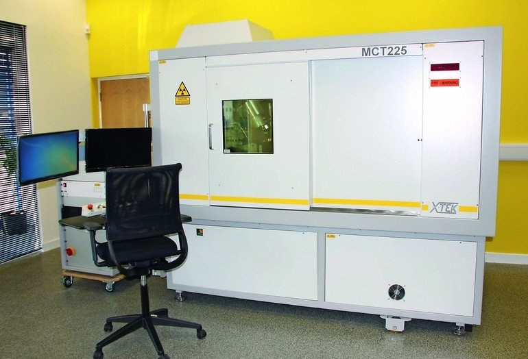
Another important feature in the portfolio is the MCT225 system. The company has successfully developed an ‘absolute accuracy’ system for metrology CT applications. It guarantees that all internal and external geometry is measured non-destructively and efficiently. It offers superior measuring accuracy and small feature detection in a 2 µm range to inspect precision plastic parts, small castings and complex parts and assemblies. A proprietary liquid cooled micro-focus reflection source and air-cooled cabinet provide long-term temperature stability and guarantee an impressive accuracy without time consuming comparative scans or reference measurements. Samples are simply placed on a rotary table inside the enclosure and measured. The 225 kV micro focus source produces incredibly sharp images with low noise levels, enabling magnification levels up to 150x.
The fully programmable, powerful 5-axis manipulator has been optimised through Finite Element Analysis (FEA). High precision linear guideways and axis travel error correction offer accurate and repeatable motion within the temperature controlled enclosure. High resolution optical encoders also fit this strategy for maximum precision. X-ray images taken by a high resolution 4-Megapixel detector is the starting point for the system’s high performance digital imaging and processing. The CT Wizard guides the operator every step of the way from sample loading to creating the final inspection report. Accelerated reconstruction of the sample volume, using optimised graphics cards, minimising the process time.
The system is an invaluable asset for manufacturers seeking to benefit from reduced lead times and inspection cycles. The powerful X-ray source and large capacity manipulator combine with high magnification and small feature detection to create a solution suited to a wide variety of applications. Moreover, the system is ideally suited for emerging production techniques, such as additive manufacturing for the production of small and highly complex components, and is able to measure these components in a single, non-destructive process. The open-tube technology of the source fitted in the system reduces the costs and allows for a quick and straightforward replacement of the filament.
There is always a demand for high performance products which are adaptable, so a good automation platform should be able to adjust to these with ease, without requiring long setup times and any special expertise. Nikon Metrology’s recently released Inspect-X 4.2 software featuring a user friendly graphical interface, where automation programs can be created without the need to code or program but use graphical icons to create a flowchart. This results less training and skill requirements to automate inspection procedures, resulting in the system to react quickly and efficiently to changing product inspection requirements.
Combining C.Clear, it provides next generation real time image enhancements, meaning that live inspection images are of the highest quality in terms of detail and clarity. C.Clear, is a key function for manufacturers looking for highest performance real-time inspection, enabling easier viewing of any defects present, as well as requiring less operator training, which would normally entail some post process image enhancement and analysis.
Real-time enhancements and filters can be chosen and stored as user profiles. Defects are detected correctly first time, especially hard to detect faults within multi-tier BGA or complex bond wires. C.Clear enables manufacturers to increase inspection throughput and to reduce false call rates, leading to improved quality and efficiency.
Nikon Metrology is constantly improving and striving to push their capabilities further, working with customers in order to meet technology demands of the future as well as production requirements of today.