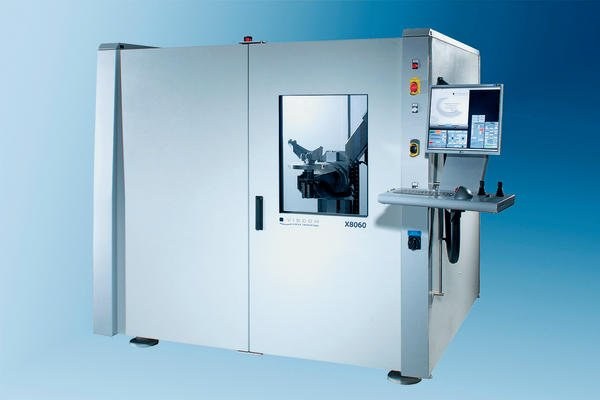
Typical defects recognized by this non-destructive process are cracks, fractures, pores, voids, foreign bodies, form deviations, incorrect positioning, misalignment or inhomogeneous material transitions. The system’s capability to inspect hidden solder joints in electronics assemblies (such as with BGAs, THDs, etc.) using high magnification and angled radiation, which allows the three-dimensional structure of the solder joints to be directly viewed and evaluated, is reportedly unique in this class of system. Its versatility makes it especially attractive to the increasing number of manufacturers who incorporate electronics into larger modules and devices.
The system’s modular precision manipulator, with up to eight CNC-capable axes, opens up new possibilities for angled irradiation with high magnification by allowing measurement in all three spatial directions, either as a two-dimensional projection or a three-dimensional volume model. High-speed processors quickly bring a realistic image of the test object to the monitor screen, where it can be sliced in any direction and analyzed.
EPP Europe 455