
Zum Inhalt springen
EPP Europe
  • News
  • Products
  • Applications
  • Technology
  • Semiconductor
  • Inspection
  • Company News
  • Events
EPP Europe
  • Technology
  • Inspection (AOI/AXI)
  • Semiconductor Packaging
  • Company News
  • Products
  • Trade Shows & Events
    EPP Europe Newsletter
    The most important electronics-manufacturing news delivered to your inbox.

    Info

    • Impressum
    • Datenschutz
    • Barrierefreiheit
    • Datenschutzeinstellungen

    Kontakt zur Redaktion

    EPP EuropeKonradin Mediengruppe
    Ernst-Mey-Str. 8, 70771 Leinfelden-Echterdingen

    E-Mail: redaktion@konradin.de
    Folgen Sie uns
    EPP Europe
    © 2026 EPP Europe
    Startseite/Semiconductor-packaging/Artikel
    Tresky offers DIE bonding prototyping and small series production
    Bildquelle nicht angegeben
    Semiconductor-packaging

    Tresky offers DIE bonding prototyping and small series production

    In the prototyping phase and when producing small series or batch size 1, many companies shy away from investing in their own Die-Bonder. Often, the final
    Veröffentlicht
    10. Juli 2022
    Lesezeit
    2 Minuten
    Rubrik
    Semiconductor-packaging

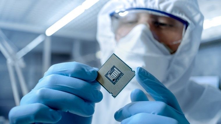
    Investments are not always made based on the respective project and development status. At the same time, many customers want to be able to produce the prototypes and small series as quickly as possible and without any loss of quality. In these cases, they rely on service providers who can take over the production of the sensitive electronic components with extensive experience and detailed knowledge. “That is why, with our technical know-how and based on our years of experience, we are now manufacturing prototypes and small series for our customers from the very first piece on our equipment. Because we can also implement all the necessary processes in our demo centre, our customers have the full manufacturing spectrum at their disposal,” says Daniel Schultze, managing owner of Tresky GmbH. In addition to epoxy/adhesive DIE bonding, Tresky offers UV DIE bonding, ultrasonic bonding (US bonding), thermocompression bonding (TC bonding), sintering, DIE stacking, flip chip bonding, DIE sorting and eutectic bonding as a service process.

    Especially in a time of high demand for components, the use of these services can be crucial for component manufacturers. That’s why Tresky helps its customers reduce time-to-market with its range of services. As an external partner, the company can also quickly produce small series on demand. On the customer’s side, it is therefore not necessary to build up additional production capacities, to use existing resources or even to interrupt series production. “This way, our customers get the products they need and can also use the production process to test the performance of our die bonders. Furthermore, we can demonstrate our reliable process capabilities. Customers thus receive an individual demonstration including a production record, which can also facilitate the decision for a machine for subsequent series production,” Schultze continues.


    Mehr aus Semiconductor-packaging

    Weitere aktuelle Artikel aus der Rubrik Semiconductor-packaging.

    Alle Semiconductor-packaging-Artikel
    Nanoscribe Expands Photoresin Portfolio for Micro-Optics Fabrication via Two-Photon PolymerizationFoto: Brecht Corbeel / Unsplash
    Semiconductor-packaging

    Nanoscribe Expands Photoresin Portfolio for Micro-Optics Fabrication via Two-Photon Polymerization

    11. November 2026

    Nanoscribe has detailed its range of photoresins engineered for Two-Photon Polymerization (2PP) and Two-Photon Grayscale Lithography (2GL), targeting high-precision micro-optics manufacturing on silicon, glass, and…

    Canon Launches FPA-6400ES6a KrF Lithography System with 400 Wafers-per-Hour ThroughputFoto: Canon Europe (semicon)
    Semiconductor-packaging

    Canon Launches FPA-6400ES6a KrF Lithography System with 400 Wafers-per-Hour Throughput

    10. November 2026

    Canon has announced the FPA-6400ES6a KrF scanner for semiconductor lithography, combining a throughput of 400 wafers per hour with industry-leading overlay accuracy of 4.0 nm and the ability to handle wafer warpage of…

    Fabmatics absorbs SCI business activities under unified brandFoto: Ludovico Ceroseis / Unsplash
    Semiconductor-packaging

    Fabmatics absorbs SCI business activities under unified brand

    6. November 2026

    Fabmatics has integrated the business activities of SCI under the Fabmatics brand, consolidating the acquired expertise within its semiconductor automation portfolio.

    Entegris and Kioxia Expand Partnership on Materials Innovation for Next-Gen 3D Flash MemoryFoto: Louis Reed / Unsplash
    Semiconductor-packaging

    Entegris and Kioxia Expand Partnership on Materials Innovation for Next-Gen 3D Flash Memory

    6. November 2026

    Entegris and Kioxia are deepening their strategic partnership to co-develop materials and process technologies for future BiCS FLASH 3D NAND architectures, using AI, digital-twin modelling and experimental validation at…

    ← Zurück zu Semiconductor-packagingZur Startseite

