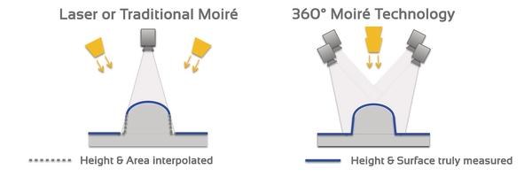
- The first issue relates to the reference used for measuring the paste height. Systems often search for a local reference near ideally on the pad, some using more than one such reference point. These can be subject to error caused by small displacement, if for example the reference point used is not actually on the pad.
- The second relates to the position and angularity corrections that must be implemented to cope with PCB warpage. This at best is time consuming, often involving mechanical movement and can cause further inaccuracies in reference measurement.
- The third relates to the frequency of fringe (or laser raster) used to generate the 3D image. The frequency determines both the range and resolution of the measurement. In order to resolve typical paste heights (In the region 100 – 120 microns) some systems only measure above a fixed height perhaps 40 micron. They assume that the area under this threshold is solid.
- The forth concern relates to the position of the orthogonal camera, which offers a 2D view from above only, necessitating some kind of imaginary construction of the side of the deposit.
- The length of time required to train the operator to use the machine. This can be particularly important where there is a high turnover of staff
- The ease of programming, as this will determine the skill set required to operate the machine, can this be done by an operator or does it require a process engineer
- The speed of programming, how long does it really take to get into production
- The cycle time (can the SPI match my line rates)
- Inspection validation, gaining confidence in the equipment and trusting the results
- And not least the reliability, accuracy and repeatability of the results.
- Gerber to pad conversion. This is usually carried out with a 3rd party software such as EPM for example. Some 3D SPI systems now offer in house data conversion. A typical example would be Sigma link which can provide front end data processing usable for both SPI and AOI machines
- Inputting of the pad data to the inspection machine.
- Input basic customer/product/batch data
- Stencil thickness input
- Fine tuning to select optimum light levels to provide maximum contrast between the solder paste and the PCB surface
- Configuring acceptable process settings. This is a task generally reserved for the process engineer with the need to set perhaps different tolerances for different pad configurations. Flexibility is usually provided to set different tolerances for different pad geometries. This can be both time and skill intensive to achieve optimum results.
- PCB load time
- Image acquisition
- Warpage correction
- Image analysis (processing)
- Results display and presentation.