Zum Inhalt springen
EPP Europe
  • News
  • Products
  • Applications
  • Technology
  • Semiconductor
  • Inspection
  • Company News
  • Events
EPP Europe
  • Technology
  • Inspection (AOI/AXI)
  • Semiconductor Packaging
  • Company News
  • Products
  • Trade Shows & Events
    EPP Europe Newsletter
    The most important electronics-manufacturing news delivered to your inbox.

    Info

    • Impressum
    • Datenschutz
    • Barrierefreiheit
    • Datenschutzeinstellungen

    Kontakt zur Redaktion

    EPP EuropeKonradin Mediengruppe
    Ernst-Mey-Str. 8, 70771 Leinfelden-Echterdingen

    E-Mail: redaktion@konradin.de
    Folgen Sie uns
    EPP Europe
    © 2026 EPP Europe
    Startseite/Technology/Artikel
    Ten-layer high density interconnect board design capability
    Bildquelle nicht angegeben
    Technology

    Ten-layer high density interconnect board design capability

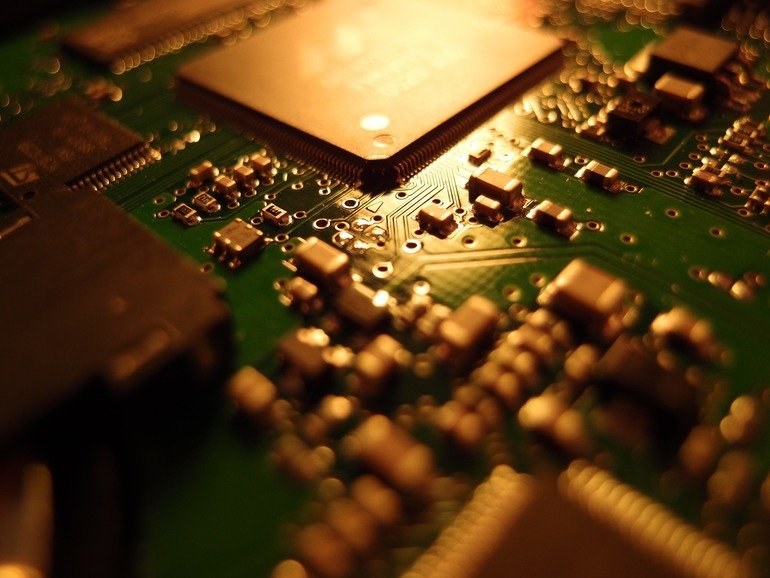
    Rush PCB Inc. offers capabilities in the design and manufacturing of multilayer High-Density Interconnect (HDI) PCBs of 10 layers and more.
    Veröffentlicht
    14. Mai 2018
    Lesezeit
    1 Minute
    Rubrik
    Technology

    Rush PCB Inc., a printed circuit design, fabrication and assembly company located in the heart of Silicon Valley, offers capabilities in the design and manufacturing of multilayer High-Density Interconnect (HDI) PCBs of 10 layers and more.

    In making the announcement, Akber Roy, CEO, stated, “To achieve very high-density interconnection, designers at Rush PCB Inc. use what we know as “Every Layer Interconnect” (ELIC) technology. This is a method wherein each layer has its own copper-filled laser-drilled micro-vias. When stacked up, it provides the opportunity for dynamic connections between any two layers in the PCB. Not only does this offer an increased level of flexibility, but it also maximizes circuit density.” Roy adds that the company’s designers have taken up the additional complex challenges in routing with Via-In-Pad (VIP) and by employing blind and buried vias. They laser-drill via holes and filled them with conductive copper paste.

    Roy adds that “Before finalizing the design of multi-layer PCBs, our designers confirm the structure of the circuit board primarily based on the scale, physical size, and the requirements of electromagnetic compatibility (EMC). Our designers use 10 layers of material, and in this ‘Stack-Up Design’ have decided that the placement of the inner layer and the manner of distribution of different signals in these layers of the multi-layer PCB. This careful planning and determination of the stack-up design beforehand save the user much time and effort in wiring and production later.”

    “Apart from very fine traces in the foil pattern, HDI requires Sequential Build-Up (SBU) and micro-vias drilled with lasers,” Roy says. “SBU technology is used to fabricate High-Density Interconnect boards. The HDI layers are usually built up from a traditionally manufactured double-sided core board or multilayer PCBs.”
    www.rushpcb.com

    Mehr aus Technology

    Weitere aktuelle Artikel aus der Rubrik Technology.

    Alle Technology-Artikel
    IPC-J-STD-002F mandates automatic flux doctor blade for solderability testingFoto: Louis Reed / Unsplash
    Technology

    IPC-J-STD-002F mandates automatic flux doctor blade for solderability testing

    10. November 2026

    The release of IPC-J-STD-002 Revision F introduces stricter, more precisely defined requirements for solderability testing, including a mandatory automatic flux doctor blade on solderability testers. Equipment lacking…

    Plasmatreat PFW10 and PFW20 Static Plasma Jets Target Sensitive PCB Surface TreatmentFoto: Johannes Plenio / Unsplash
    Technology

    Plasmatreat PFW10 and PFW20 Static Plasma Jets Target Sensitive PCB Surface Treatment

    28. Oktober 2026

    Plasmatreat's PFW10 and PFW20 static plasma jet systems are designed for selective, high-accuracy surface treatment of sensitive electronic assemblies, including circuit boards, using cold atmospheric-pressure plasma.

    Indium Corporation to Present High-Reliability Solder Pastes at EFX 2026 in StuttgartFoto: Indium Corporation
    Technology

    Indium Corporation to Present High-Reliability Solder Pastes at EFX 2026 in Stuttgart

    30. September 2026

    Indium Corporation will exhibit three solder paste technologies at Expo for Electronics Manufacturing (EFX) 2026 in Stuttgart, Germany, addressing thermal cycling performance, low-temperature step soldering and…

    Europlacer: Software as the Core Performance Driver in High-Mix SMTFoto: Brecht Corbeel / Unsplash
    Technology

    Europlacer: Software as the Core Performance Driver in High-Mix SMT

    24. September 2026

    Europlacer makes the case that traditional SMT software was not designed for the demands of high-mix, short-run production, and that the resulting performance gap is increasingly visible on the shop floor.

    ← Zurück zu TechnologyZur Startseite