
» Siegfried Lorenz, Indium Corporation, and Andreas Prusak, Panasonic Factory Solutions Europe
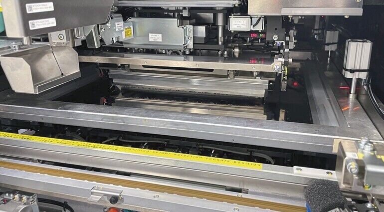
Panasonic’s Paper-free Wiping Unit, developed for the company’s stencil printers, innovatively uses multi aligned blades instead of traditional cleaning paper. New possibilities emerge when the unit is combined with Indium Corporation’s Indium8.9HFRV high-performance solder paste.
Paperless cleaning
The miniaturization of components and electronics continues to progress. To ensure optimal and reproducible printing results, a clean stencil during operation is crucial. To meet these challenges on the materials side, solder paste is becoming increasingly fine. The solder paste used for the DoE (Design of Experiments) was type 5, with a powder size between 15 and 25 µm. Indium Corporation also produces powders up to type 8.
The Paper-free Wiping Unit integrates seamlessly into manufacturing environments, allowing customers to meet the growing demands of miniaturized electronics. The unit features a patented cleaning mechanism that effectively removes residual solder paste and debris from the stencil underside without the use of consumable paper. By combining a vacuum-assisted cleaning head and a solvent application system, the unit achieves reliable cleanliness even for challenging stencils, such as those with fine-pitch apertures or step-down designs. This innovative solution not only supports sustainability goals but also reduces maintenance requirements, enhancing operational efficiency. Stencil printers equipped with this unit are designed for easy integration into smart factory setups, ensuring compatibility with Industry 4.0 standards.
During the DoE, the companies’ engineers used a demo board with various pads at Panasonic’s facility in Ottobrunn to reflect the components and apertures typically used by customers. The 100 µm stencil, which included a step-down to 80 µm, posed no challenges. Additionally, apertures with an area ratio of 0.58 were implemented in the stencil and successfully printed, demonstrating the excellent transfer efficiency of Indium8.9HFRV.
Engineered for advanced applications, the solder paste offers superior printing performance and reliability. It features an enhanced flux system that ensures excellent wetting properties and consistent transfer efficiency, even for apertures with area ratios below 0.66. It delivers stable performance across a wide range of printing conditions, reducing the need for frequent process adjustments. The paste’s low voiding characteristics and high oxidation resistance make it an ideal choice for modern electronic assemblies.
Following the setup of the stencil printer, all relevant parameters were measured using a Koh Young SPI, both for cleaning with paper and liquid cleaner and with the Paper-free Wiping Unit. Cleaning was performed at the start and after every third board. Transfer efficiency, which indicates the volume of solder paste transferred as a percentage, was used as an indicator of stencil underside cleanliness. The only variable during the DoE was the cleaning unit. The data shows minimal differences in printing performance, which can be attributed to the proven performance of Indium8.9HFRV. As a result, costs for cleaning paper and liquid cleaner are reduced. In a 24-hour operation, the consumption amounts to 13 km/year if the cycle time per PCB is 30 seconds and cleaning occurs after every three cycles.
Additionally, time savings were observed. While a paper cleaning cycle takes around 25 seconds, paperless cleaning is approximately 10 seconds faster per cycle, increasing output by approximately 9%. This calculation does not account for the time saved by avoiding paper roll changes, which also eliminates potential sources of error.
Panasonic’s engineers also note that the unit contributes to a cleaner working environment by eliminating the need to handle used cleaning paper rolls, which often contain solder paste residues. This innovation not only minimizes waste but also enhances operator safety by reducing direct exposure to cleaning solvents. Furthermore, the company has integrated advanced monitoring capabilities into its stencil printers, enabling real-time tracking of cleaning performance and system diagnostics. These features ensure consistent quality and provide valuable insights for process optimization.
The solder paste further complements these advancements with its environmental credentials. Being formulated with halogen-free flux, it meets stringent environmental regulations without compromising performance. Its compatibility with various cleaning methods underscores its versatility and adaptability to evolving manufacturing needs.
Setting a new standard
The test results highlight the importance of effective stencil underside cleaning during operation. The combination of Indium Corporation’s Indium8.9HFRV solder paste with Panasonic‘s Paper-free Wiping Unit is not only sustainable but also facilitates further automation, eliminating error-prone aspects of paper-based cleaning systems and setting a new standard for stencil printing processes. This collaboration demonstrates how forward-thinking solutions can address the challenges of modern electronics manufacturing while promoting sustainability and efficiency. As the industry continues to evolve, these advancements will play a pivotal role in shaping the future of stencil printing technology.



