Zum Inhalt springen
EPP Europe
  • News
  • Products
  • Applications
  • Technology
  • Semiconductor
  • Inspection
  • Company News
  • Events
EPP Europe
  • Technology
  • Inspection (AOI/AXI)
  • Semiconductor Packaging
  • Company News
  • Products
  • Trade Shows & Events
    EPP Europe Newsletter
    The most important electronics-manufacturing news delivered to your inbox.

    Info

    • Impressum
    • Datenschutz
    • Barrierefreiheit
    • Datenschutzeinstellungen

    Kontakt zur Redaktion

    EPP EuropeKonradin Mediengruppe
    Ernst-Mey-Str. 8, 70771 Leinfelden-Echterdingen

    E-Mail: redaktion@konradin.de
    Folgen Sie uns
    EPP Europe
    © 2026 EPP Europe
    Startseite/Applications/Artikel
    Solution for materials management and imaging
    Bildquelle nicht angegeben
    Applications

    Solution for materials management and imaging

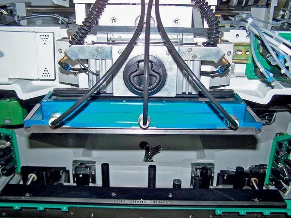
    The M3i from DEK is a process-enabling system that provides turnkey materials management and printing capabilities heretofore unavailable, enabling high
    Veröffentlicht
    19. September 2007
    Lesezeit
    2 Minuten
    Rubrik
    Applications

    “There are many, many applications that will benefit from DEK’s M3i technology,” states Neil MacRaild, DEK Americas General Manager. “Right now, for example, we are working with a leading semiconductor firm on an encapsulation application and, frankly, producing this product in high volume would not be possible without the M3i system. The possibilities for enabling new processes are endless.” The versatility of the system allows for materials to be stored in the cartridges at low temperature and then heated within the enclosed print head when elevated materials temperatures or melting processes are required. With the ability to control a variety of materials conditions – from temperature to metering to mix ratios – for unlimited volumes of material, the new system is an enabling technology for high-volume production environments where efficient materials management is essential.

    It is completely scalable and can be used for numerous applications including, but not limited to: Underfill, encapsulation, solar cell and fuel cell imaging and many other packaging processes. As the system operates in real- time and is fully automated and programmable, throughput is vastly improved, errors introduced by operator intervention are eliminated, waste is reduced and significant cost savings are realized.

    www.dek.com

    EPP Europe 441

    Mehr aus Applications

    Weitere aktuelle Artikel aus der Rubrik Applications.

    Alle Applications-Artikel
    Expert to highlight new solder paste in Rosemont
    Applications

    Expert to highlight new solder paste in Rosemont

    25. August 2025

    AIM Solder is participating in the upcoming SMTA International 2025 event, which is taking place from October 19–23 at the Donald E. Stephens Convention

    Selective soldering machine take production to a new level
    Applications

    Selective soldering machine take production to a new level

    27. Mai 2025

    Under the motto “Assembling the Future”, Phonotronica Ltd. has been a pioneer in the development and manufacture of electronic modules since 1990.

    ← Zurück zu ApplicationsZur Startseite