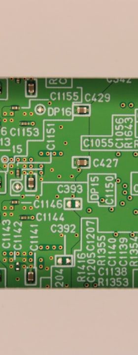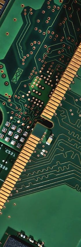
The continued coexistence of through-hole technology (THT) and surface-mount technology (SMT) on the same printed circuit board is a practical reality in sectors ranging from automotive electronics to industrial control systems. While wave soldering has historically served as the standard process for THT joints, the growing density of modern assemblies and the increasing use of heat-sensitive SMD components on the secondary side have created conditions under which wave soldering is no longer viable without masking. Selective soldering addresses this constraint directly: by applying molten solder only to precisely defined locations on a board, it eliminates the need for solder masks or pallets in many applications and reduces thermal exposure across the assembly.
Unlike reflow soldering, which is a fundamentally batch-oriented thermal process acting on an entire board simultaneously, selective soldering is an additive, point-by-point or zone-by-zone operation. This distinction has direct implications for process design, throughput calculation and defect prevention strategies.
Process Variants: Laser, Mini-Wave and Drag Soldering
Three principal process variants are in industrial use. The mini-wave process, the most widely deployed, uses a small nozzle — typically between 3 mm and 10 mm in diameter — through which solder is pumped to form a controlled, localised wave. The board, held by an XY positioning system or a gantry, moves the target joint over this wave. Nozzle geometry, solder alloy, contact time, board speed and immersion depth are the primary process variables.
Drag soldering is a variant in which the nozzle moves beneath the stationary or slowly advancing board, drawing a trail of solder along a row of joints — for example, a connector pin row. It offers higher throughput for linear patterns but is less flexible when joint positions are scattered across the board. Laser-based selective soldering, though less common in high-volume production, uses a focussed laser beam to heat the joint while solder wire is fed from the side. Its very localised energy input makes it suitable for thermally fragile assemblies, but capital costs and process complexity are considerably higher.
Flux Application: The Critical Precursor Step
Because selective soldering acts on individual joints rather than an entire board surface, flux application must be equally selective. Three methods are common: drop-jet fluxing, spray fluxing with a micro-nozzle, and pin-transfer fluxing. Drop-jet systems, analogous in principle to inkjet printing, deposit discrete flux droplets at programmed coordinates and offer the highest positional accuracy, typically within ±0.1 mm. This is particularly important when flux exclusion zones — areas where flux residues would compromise electrical performance or adhesion of conformal coatings — are present nearby.
Flux type selection must align with residue management requirements. No-clean fluxes are widely used to avoid a downstream cleaning step, but the residue volume deposited by selective fluxers is typically higher per joint than in wave soldering, which can create issues with in-circuit test probe contact or optical inspection. If the assembly must be conformal-coated, compatibility between flux residue chemistry and coating material requires explicit validation.
Thermal Management: Preheating and Heat Balance
Adequate preheating is not optional in selective soldering — it is a process-critical requirement. Insufficient preheat leads to thermal shock in board substrates, incomplete flux activation, cold joints and, in extreme cases, delamination of multilayer boards. Standard preheating modules in selective soldering systems use infrared emitters, convection heaters or a combination of both, typically bringing the bottom side of the board to between 90 °C and 130 °C before the solder contact phase.
The heat balance at the joint itself is determined by the interaction between incoming solder temperature (commonly 265 °C to 285 °C for Sn-Ag-Cu alloys), contact time, nozzle diameter, and the thermal mass of the component lead and pad. Boards with heavy ground planes or large-diameter copper pours require longer dwell times or higher solder temperatures to achieve adequate wetting. Process engineers must construct a defined process window for each board design, verifying wetting angles, hole fill percentages and joint morphology against IPC-A-610 acceptance criteria.
Solder Alloy Considerations and Nozzle Maintenance
The solder reservoir in a selective soldering system is a relatively small bath compared to a wave solder machine, which means the ratio of dissolved copper and other contaminants to total solder volume can rise quickly if maintenance intervals are neglected. Copper dissolution from PCB pads and component leads is ongoing during operation. Regular dross removal and periodic alloy analysis — checking copper, silver, tin and impurity concentrations against IPC J-STD-001 limits — are essential for maintaining joint quality over time.
Nozzle geometry and surface condition directly affect wave stability and wetting behaviour. Oxidised or partially blocked nozzles cause wave turbulence, solder bridging and inconsistent joint volumes. Most equipment manufacturers recommend nozzle inspection after every production shift and replacement or chemical cleaning according to a defined schedule. Titanium nozzles offer improved resistance to dissolution and corrosion compared to steel variants and are the current industry standard for lead-free alloys.
Inspection Strategies and Process Qualification
Post-selective-solder inspection presents specific challenges. The recessed geometry of many THT joints — particularly when surrounded by tall components — limits the angle of view for standard 2D automated optical inspection (AOI) systems. Angled multi-camera AOI, 3D AOI and X-ray inspection (AXI) are increasingly deployed in line directly after the selective soldering module. AXI is particularly valuable for assessing hole fill, which cannot be evaluated from the topside surface alone and which is a mandatory criterion under IPC-A-610 for class 2 and class 3 assemblies.
Process qualification for selective soldering should follow a structured design-of-experiments (DOE) approach, systematically varying contact time, solder temperature, flux deposit volume and preheat temperature to map the process window. First-article inspection results, including cross-sectional analysis of representative joints, establish the baseline. Statistical process control (SPC) monitoring of key parameters — solder bath temperature, flux deposit weight, nozzle dwell time — then provides ongoing assurance that the process remains within the validated window during series production.
Integration into MES and Traceability Architectures
Modern selective soldering systems communicate via standardised machine interfaces — increasingly based on the IPC-HERMES-9852 board transport protocol and IPC-CFX (Connected Factory Exchange) — enabling full integration into manufacturing execution systems. Each board's process data record can include nozzle coordinates, actual solder temperatures, contact durations and flux deposit confirmations, linked to the board serial number for end-to-end traceability. This data infrastructure is not merely a compliance tool: it enables rapid root-cause analysis when field returns occur and supports continuous process optimisation through systematic analysis of parameter drift against yield trends.
As assembly densities continue to increase and the mix of THT and SMT components on individual boards becomes more complex, selective soldering will remain an indispensable process technology. Mastery of its fundamental variables — flux chemistry and deposition accuracy, preheat adequacy, solder alloy management and nozzle condition — combined with rigorous inline inspection and data-driven process monitoring, determines whether the technology delivers its potential for high joint quality with minimal thermal risk to surrounding components.