Due to the difference in the heat capacity ratio between the board and components, the reflow conditions at the solder joint will vary in melting temperature, time, and cooling rate. This means the joint structure may not be identical, partly due to the metal diffusion from the board and component.
Reflow soldering process is prominent for mobile electronics, especially for miniaturizing components, such as in 2.5D and 3D assembly. It is also important for automotive electronics due to the use of increasingly dense assemblies, such as a safety package for automated driving. This article shows the inevitable influence of the varying reflow conditions on the solder joint structure, and presents the results of verification performed with SAC305.
Preparation of the test board
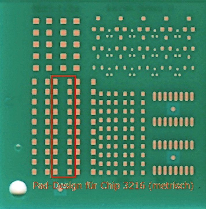
The test board was made with the use of a SAC305 alloy composition solder paste, 3216 metric size chip resistors, and substrate. The thickness of the stencil was 120 µm. SK-5000, a high temperature observation equipment by Sanyo Seiko, was used for reflow, in a N2 environment.
Preparation of test sample
The test board was cut in the perimeter of 3216 metric size chip resistor. The cutout was then sealed with heat-curing encapsulation resin, and grinded to the center of the encapsulated chip component, after it was cured to make the test sample for observation.
Varying peak temperatures
The Sn phase coarsened in the solder joint structure with all surface finishes obtained via the reflow profiles while the peak temperature was at or less than 240 °C. The coarse IMC, presumably Cu6Sn5, was observed in the solder structure with all finishes except for ENIG, via the reflow profile with the peak temperature at 270 °C. It is possible that the IMC was formed due to a dispersion of copper from the test board.
Varying melting times
There was no major difference seen in the Sn phase within the solder joint structure that was obtained via reflow profiles, when the melting time was the standard 45 seconds or longer. However, when the melting time was longer, it resulted in a smaller Sn-Ag eutectic phase and the formation of Ag3Sn IMC.
Varying cooling rates
The solder joint structures obtained via reflow profiles with the different cooling rates were interesting to measure. The cooling rate of or below –2.0 °C/sec, resulted in the coarsened Sn phase, smaller Sn-Ag eutectic phase, and coarsening of presumably Cu6Sn5 IMC for all surface finishes.
Conclusion
Findings from the evaluation of the effects of different reflow profile conditions are as follows:
- When the peak temperature of a reflow profile was at or below 240°C, the Sn phase coarsened in the solder structure. At or above 270 °C, the coarse IMC, presumably Cu6Sn5, precipitated when using the boards without Cu barrier.
- Time exceeding 45 seconds that was above the reflow peak temperature resulted in a smaller Sn-Ag phase and precipitation of Ag3Sn.
- When the cooling rate was at or less than –2 °C/sec., the Sn phase coarsened, Sn-Ag eutectic phase dwindled, and IMC of presumably Su6Sn5 crystalized in the solder joint structure.
Further discussion
A customer once asked the company, Koki, to analyze an assembly soldered with SAC305 alloy that failed after less than 1000 thermal cycles. As a result of analysis, the company found that the BGA joint of a module substrate inside the shield case was fractured.
In the fractured solder joint structure, the coarsening of Sn phase and the IMC was observed. At the time, the cause could not be identified, since the number of thermal cycles and the state of solder structure did not seem to be correlated. However, examining the results above, the company can now make an assumption that the solder joint structure was similar to that of a low-silver containing solder joint because it was slowly cooled inside the high heat capacitance shield case.
A further investigation into the influences on the thermal cycling durability by the differences in solder joint structure will be done, to prove that not only is the alloy composition important, but the temperature conditions are also very important to improve the durability of solder joint.
Zusammenfassung Résumé Zusammenfassung russisch
Dieser Artikel berichtet über den unvermeidlichen Einfluss der unterschiedlichen Reflow-Bedingungen auf die Lötstellenstruktur und stellt die Ergebnisse der Überprüfung nach der Implementierung mit SAC305 vor.
Cet article rapporte l‘impact inévitable de différentes conditions de refusion sur la structure de joint de soudure et présente les résultats de la vérification post-implémentation (après la mise en œuvre) avec SAC305.
Эта статья рассказывает о неизбежном влиянии различных условий оплавления припоя на структуру точки пайки и представляет результаты проверки после внедрения SAC305.