
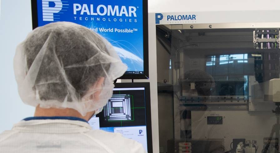
Palomar Technologies, a global leader in total process solutions for advanced photonics and microelectronic device packaging today announced the availability of their new Palomar 3880-II Die Bonder. The new Palomar 3880-II die bonder is based on Palomar’s proven 3880 die bonder design but now includes options to even further maximize productivity, reduce programming time by up to 95% and improve the overall bonder productivity.
“We are excited to launch this upgraded version of our long-standing, flexible die bonder. The new Palomar 3880-II Die Bonder builds upon the proven engineering of our previous bonders in the Palomar family, the Palomar 3500, 3800 and 3880 die bonders,” said Rich Hueners, Vice President of Sales and Marketing for Palomar Technologies. “Users of the 3880-II can expect the same unparalleled flexibility in the 3880-II with support for eutectic, epoxy, solder paste, inspection, tracking, sorting, all in one machine that can continually scale up in automation and volume. It represents a solid investment for all customers from R&D up to volume, automated bonding.”
The Palomar 3880-II Die Bonder maximizes productivity with a number of improvements, including:
- Support for rapid process development that minimizes gaps in production caused by maintenance, calibrations, and process set-ups.
- Simultaneously supports multiple types of processes, automation equipment and custom systems with all equipment installed in one large work envelope.
- A new tool changer providing automated access to nearly unlimited tools.
- Palomar’s Vision Standardization™ software that calibrates images between different Palomar bonding systems, dramatically eliminating the time and cost associated with maintaining programs across multiple systems and numerous programs on a system over time.
- A smart tray feeder that saves space for high mix, highly complex environments that can present up to 180 unique components simultaneously.
- A new contactless height measurement for quick and precise height measurement.
- Improved force range with both precision low forces and robust forces up to 10kg
Additionally, the 3880-II can reduce programming time by up to 95% with:
- Simplified process creation for even the most complex assemblies with offline programming to import data from CAD designs.
- Expedited program creation through easy to use software with simple component source location definitions.
- Graphical tools that speed up process creation and provide easy to understand feedback.
- Support to utilize any previously defined data from across machines to quickly build up complex assemblies.
The highly flexible Palomar 3880-II is ideally suited for a range of markets and applications by providing a large work envelope with an open platform for hardware mounting. Typical applications for the Palomar 3880-II Die Bonder include:
- AOC – Active optical cable
- Chip-on-board
- CMOS sensors
- GaN/GaAs MMIC
- HB/HP LED assembly
- HPLD (high power laser diode)
- Hybrid microcircuits
- LiDAR
- Medical semiconductor & sensors
- MEMS / MOEMS
- Microwave modules
- Power electronics
- Quantum computing
- RF GaN 5G power amplifiers
- RF packages
- RF power amplifier
- VCSEL, PD, DFB Laser, Lens Attach
For more information on the Palomar 3880-II Die Bonder, visit: Palomar 3880-II Die Bonder.
About Palomar
Technologies Palomar Technologies makes the connected world possible by delivering a Total Process Solution™ for advanced photonic and microelectronic device assembly processes utilized in today’s smart, connected devices. With a focus on flexibility, speed and accuracy, Palomar’s Total Process Solution includes Palomar die bonders, Palomar wire and wedge bonders, SST vacuum reflow systems, along with Innovation Centers for outsourced manufacturing and assembly, and Customer Support services, that together deliver improved production quality and yield, reduced assembly times, and rapid ROI.
With its deep industry expertise, Palomar equips customers to become leaders in the development of complex, digital technologies that are the foundation of the connected world and the transmission of data generated by billions of connected devices. Palomar solutions are utilized by the world’s leading companies providing solutions for Datacom, 5G, electric vehicle power modules, autonomous vehicles/LiDAR, enhanced mobile broadband, Internet of Things, SMART technology, and mission critical services.
Headquartered in Carlsbad, California, Palomar offers global sales, service and application support from its offices in the USA, Germany, Singapore and China.



