Zum Inhalt springen
EPP Europe
  • News
  • Products
  • Applications
  • Technology
  • Semiconductor
  • Inspection
  • Company News
  • Events
EPP Europe
  • Technology
  • Inspection (AOI/AXI)
  • Semiconductor Packaging
  • Company News
  • Products
  • Trade Shows & Events
    EPP Europe Newsletter
    The most important electronics-manufacturing news delivered to your inbox.

    Info

    • Impressum
    • Datenschutz
    • Barrierefreiheit
    • Datenschutzeinstellungen

    Kontakt zur Redaktion

    EPP EuropeKonradin Mediengruppe
    Ernst-Mey-Str. 8, 70771 Leinfelden-Echterdingen

    E-Mail: redaktion@konradin.de
    Folgen Sie uns
    EPP Europe
    © 2026 EPP Europe
    Startseite/Products/Artikel
    New test methods
    Bildquelle nicht angegeben
    Products

    New test methods

    Apart from the layout and housing design, the characteristics of the ICs used play a key role for the EMC characteristics of devices. Reducing the size of
    Veröffentlicht
    22. Oktober 2015
    Lesezeit
    1 Minute
    Rubrik
    Products
    • identify EMC problems in the device on the IC level
    • select ICs on the basis of the gained insights and
    • optimise the circuit and/or layout design to the EMV parameters of ICs.
    • measure and check the immunity of/emissions from ICs
    • identify the causes of interference and
    • optimise the ICs
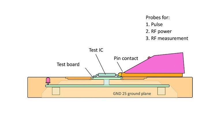
    • a test board for the test IC which provides a uniform interface between the test IC and test system
    • a CB 0708 connection board which is used to trigger the test IC
    • a GND25 ground plane which provides a uniform reference potential
    • a disturbance generator (e.g. EFT/burst)
    • an oscilloscope
    • a spectrum analyzer
    • a PC
    • a power amplifier
    • The induced voltage affects the IC’s pin that is switched as the input. The disturbance voltage uSt is converted into a spurious signal in the IC by the input circuit and further processed as a logic signal.
    • The induced voltage drives a disturbance current iSt into the pins of the IC. This disturbance current enters the IC’s internal Vdd/Vss system directly if these are the Vdd/Vss pins. However, it can also enter via signal pins and be led to the Vdd/Vss system inside the IC via internal drivers or protective diodes or capacitances. The Vdd/Vss system passes the disturbance current on to other functional components of the IC so that malfunctions can arise in areas that are not functionally connected to the affected pins.
    • The network essentially has circuit elements R, L and diodes against Vdd and Vss on the board and in the IC. The displacement current generates a disturbance pulse uSt at these elements. This disturbance pulse is converted into a spurious signal in the IC by the input circuit and further processed as a logic signal.
    • The displacement current is split into two shares. The first share is discharged via the equivalent circuits of the board and any decoupling capacitors that may be present. The second share of the disturbance current iSt flows through the IC via drivers or protective diodes to the Vdd/Vss system. It produces effects similar to those of a magnetic field coupling.

    Mehr aus Products

    Weitere aktuelle Artikel aus der Rubrik Products.

    Alle Products-Artikel
    Heavy board options added to reflow soldering system
    Products

    Heavy board options added to reflow soldering system

    27. Mai 2025

    Provider of reflow soldering technology, Vitronics Soltec has launched new Heavy Board options for its Centurion 1240 reflow soldering system. This

    New 3D AXI platform provides clearer imaging
    Products

    New 3D AXI platform provides clearer imaging

    22. Januar 2025

    Test Research, Inc. (TRI) has announced the launch of its new 3D AXI TR7600FB SII system and emphasized that it has been designed to deliver clearer

    No-clean formula maximize the solderability
    Products

    No-clean formula maximize the solderability

    10. Januar 2025

    Indium Corporation announced the global availability of CW-807RS, a new high-reliability, halide- and halogen-free flux-cored wire that improves wetting

    Extensive program of testing options
    Products

    Extensive program of testing options

    10. Januar 2025

    Test Research, Inc. (TRI) will join the IPC APEX EXPO 2025 held at Anaheim Convention Center on March 18 – 20, 2025 at booth #2905 to show latest test and

    ← Zurück zu ProductsZur Startseite