Zum Inhalt springen
EPP Europe
  • News
  • Products
  • Applications
  • Technology
  • Semiconductor
  • Inspection
  • Company News
  • Events
EPP Europe
  • Technology
  • Inspection (AOI/AXI)
  • Semiconductor Packaging
  • Company News
  • Products
  • Trade Shows & Events
    EPP Europe Newsletter
    The most important electronics-manufacturing news delivered to your inbox.

    Info

    • Impressum
    • Datenschutz
    • Barrierefreiheit
    • Datenschutzeinstellungen

    Kontakt zur Redaktion

    EPP EuropeKonradin Mediengruppe
    Ernst-Mey-Str. 8, 70771 Leinfelden-Echterdingen

    E-Mail: redaktion@konradin.de
    Folgen Sie uns
    EPP Europe
    © 2026 EPP Europe
    Startseite/Products/Artikel
    New paths in metallisation for the areas SMT, solar and hybrid technology
    Bildquelle nicht angegeben
    Products

    New paths in metallisation for the areas SMT, solar and hybrid technology

    M-TeCK is the new metallisation technology of Christian Koenen. It comprises special stencils, squeegees, cleaning materials and processes. For the areas
    Veröffentlicht
    02. November 2012
    Lesezeit
    1 Minute
    Rubrik
    Products
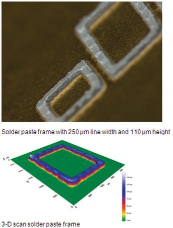
    • SMT – Adaptation to substrate surfaces and complex structures: The elastic characteristics of the stencil allow for the printing of substrates with significant surface waviness, which cannot be printed using conventional stainless steel stencils. Applications include extreme multilayer substrates that display variations in thickness and height after pressing. The elastic sealing properties of the stencil are significantly enhanced by the additional coating. As a result, this process can be used for compensating local height variations. With the extended design options offered by the M-TeCK stencil, it is possible to print closed frames and other complex structures. For example, printing of a closed paste frame ensures optimal wetting of HF frames.
    • Solar cell printing: Thanks to its special characteristics, the M-TeCK stencil allows printing of fine lines with an optimal cross-section for the power line. With the high positioning accuracy, promising processes such as selective emitters can be implemented efficiently.
    • Hybrid technology – Fine lines and even surfaces: Thanks to the complex freedom of design, it is possible to produce layouts with fine lines and large areas. Low or high film thicknesses can be produced for print areas and unlike in screen printing, this can be implemented in a single printing process. Significant process improvements and time savings can be achieved in particular for high power applications.

    Mehr aus Products

    Weitere aktuelle Artikel aus der Rubrik Products.

    Alle Products-Artikel
    Heavy board options added to reflow soldering system
    Products

    Heavy board options added to reflow soldering system

    27. Mai 2025

    Provider of reflow soldering technology, Vitronics Soltec has launched new Heavy Board options for its Centurion 1240 reflow soldering system. This

    New 3D AXI platform provides clearer imaging
    Products

    New 3D AXI platform provides clearer imaging

    22. Januar 2025

    Test Research, Inc. (TRI) has announced the launch of its new 3D AXI TR7600FB SII system and emphasized that it has been designed to deliver clearer

    No-clean formula maximize the solderability
    Products

    No-clean formula maximize the solderability

    10. Januar 2025

    Indium Corporation announced the global availability of CW-807RS, a new high-reliability, halide- and halogen-free flux-cored wire that improves wetting

    Extensive program of testing options
    Products

    Extensive program of testing options

    10. Januar 2025

    Test Research, Inc. (TRI) will join the IPC APEX EXPO 2025 held at Anaheim Convention Center on March 18 – 20, 2025 at booth #2905 to show latest test and

    ← Zurück zu ProductsZur Startseite