
Skip to content
EPP Europe
  • News
  • Technology
  • Semiconductor
  • Inspection
  • Company News
  • Events
  • Expert Forum
EPP Europe
  • Technology
  • Inspection (AOI/AXI)
  • Semiconductor Packaging
  • Company News
  • Products
  • Trade Shows & Events

Info

  • Legal notice
  • Privacy
  • Accessibility
  • Privacy settings

Editorial contact

EPP EuropeKonradin Mediengruppe
Ernst-Mey-Str. 8, 70771 Leinfelden-Echterdingen

E-Mail: redaktion.eppe@konradin.de
Follow us
EPP Europewirautomatisierer.debatterie-produktion.deKunststoff-Reportdeutsche-ernaehrungsindustrie.depharma-prozesstechnik.de
© 2026 EPP Europe
Home/Semiconductor Packaging/Article
Nanoscribe Expands Photoresin Portfolio for Two-Photon Grayscale Lithography
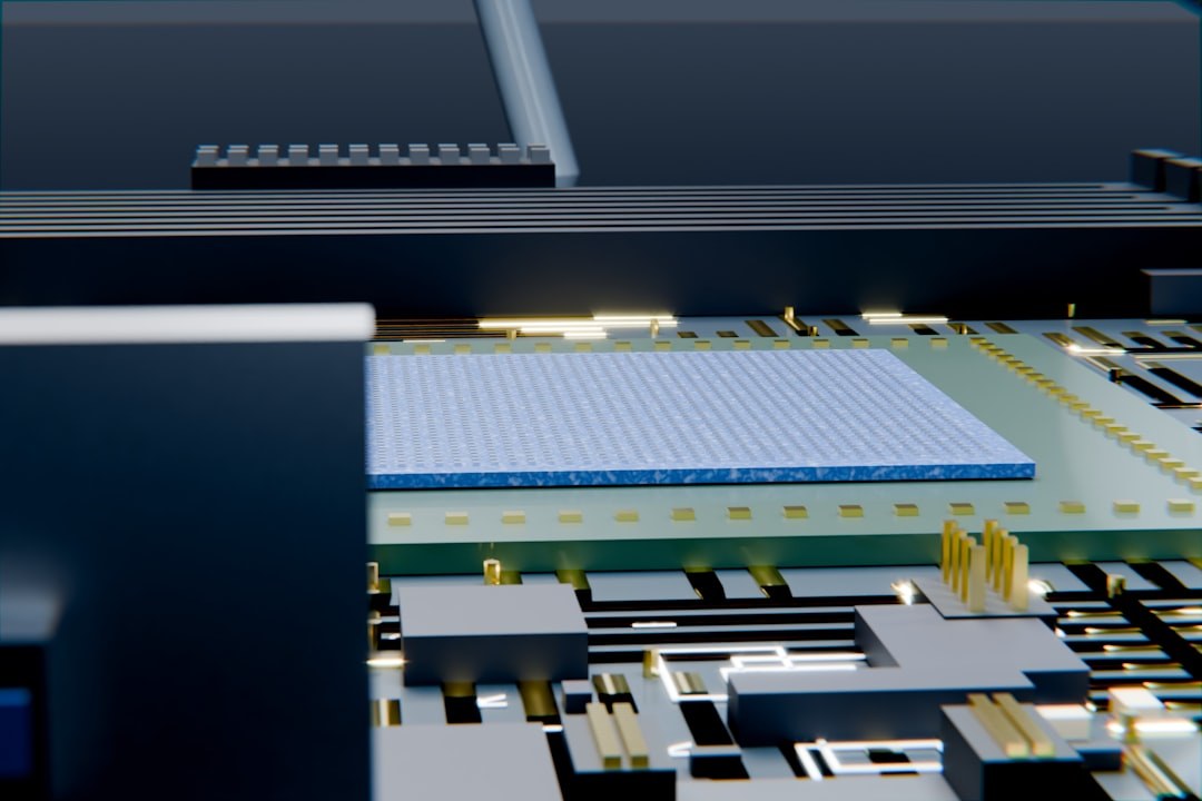
Foto: Brecht Corbeel / Unsplash
Semiconductor Packaging

Nanoscribe Expands Photoresin Portfolio for Two-Photon Grayscale Lithography

Five industrial-grade resins now available with batch-specific Certificates of Analysis for 2.5D surface patterning applications
Published
19 November 2026
Reading time
1 minute
Section
Semiconductor Packaging

Nanoscribe offers five photoresins specifically formulated for Two-Photon Grayscale Lithography (2GL), addressing requirements in 2.5D surface patterning such as low volume shrinkage, high two-photon sensitivity, and smooth surface finishes. The lineup comprises IPX-Clear, IP-S, IP-Dip2, IPX-S, and OrmoComp — the latter supplied by micro resist technology. All materials are qualified for nanoimprint lithography (NIL) and micro injection molding (µIM), with reliable demolding behaviour to support high-quality replica production.

The five most in-demand resins are now manufactured to industrial-grade material quality and ship with batch-specific Certificates of Analysis (CoAs), a step relevant for process traceability in semiconductor and advanced packaging workflows. Applications include diffractive optical elements (DOEs), nanophotonics structures, and replication masters for volume production. Strong adhesion to silicon, glass, and further substrates, combined with mechanical stability, is cited as enabling reproducible results across direct fabrication and master template manufacturing.

Quelle: Nanoscribe (semicon) – https://www.nanoscribe.com/en/products/surface-patterning-2pp-printing-materials/

More from Semiconductor Packaging

More recent articles from Semiconductor Packaging.

All articles from Semiconductor Packaging
PHIX and Nanoscribe Offer Photonics Packaging Service for Lensed Fiber ArraysFoto: Nanoscribe (semicon)
Semiconductor Packaging

PHIX and Nanoscribe Offer Photonics Packaging Service for Lensed Fiber Arrays

18 November 2026

PHIX B.V. and Nanoscribe have launched a commercial photonics packaging and assembly service producing lensed fiber arrays via Aligned 2-Photon Lithography, targeting photonic integrated circuit coupling and optical…

Advantest expands V93000 EXA Scale platform with new EXA Scale QX test headFoto: Advantest
Semiconductor Packaging

Advantest expands V93000 EXA Scale platform with new EXA Scale QX test head

18 November 2026

New test head extends platform scalability to address high-power and high-pin-count applications.

Nanoscribe scales photoresin manufacturing to industrial gradeFoto: Nanoscribe (semicon)
Semiconductor Packaging

Nanoscribe scales photoresin manufacturing to industrial grade

18 November 2026

Nanoscribe has invested in expanded manufacturing capabilities for five widely used photoresins, introducing industrial-grade quality standards and batch-specific CoA documentation to support growing adoption in optics…

Plasmatreat Presents Coordinated Plasma Portfolio for Semiconductor Surface Conditioning at SEMICON Europa 2026Foto: Plasmatreat (semicon)
Semiconductor Packaging

Plasmatreat Presents Coordinated Plasma Portfolio for Semiconductor Surface Conditioning at SEMICON Europa 2026

16 November 2026

At SEMICON Europa in Munich, Plasmatreat demonstrates how combining multiple plasma technologies enables controlled, reproducible surface conditions across advanced chip and packaging processes — from oxide reduction on…

← Zurück zu Semiconductor PackagingTo the homepage