
Skip to content
EPP Europe
  • News
  • Technology
  • Semiconductor
  • Inspection
  • Company News
  • Events
EPP Europe
  • Technology
  • Inspection (AOI/AXI)
  • Semiconductor Packaging
  • Company News
  • Products
  • Trade Shows & Events

Info

  • Legal notice
  • Privacy
  • Accessibility
  • Privacy settings

Editorial contact

EPP EuropeKonradin Mediengruppe
Ernst-Mey-Str. 8, 70771 Leinfelden-Echterdingen

E-Mail: redaktion.eppe@konradin.de
Follow us
EPP Europewirautomatisierer.debatterie-produktion.deKunststoff-Reportdeutsche-ernaehrungsindustrie.depharma-prozesstechnik.de
© 2026 EPP Europe
Home/Semiconductor Packaging/Article
Advantest expands V93000 EXA Scale platform with new EXA Scale QX test head
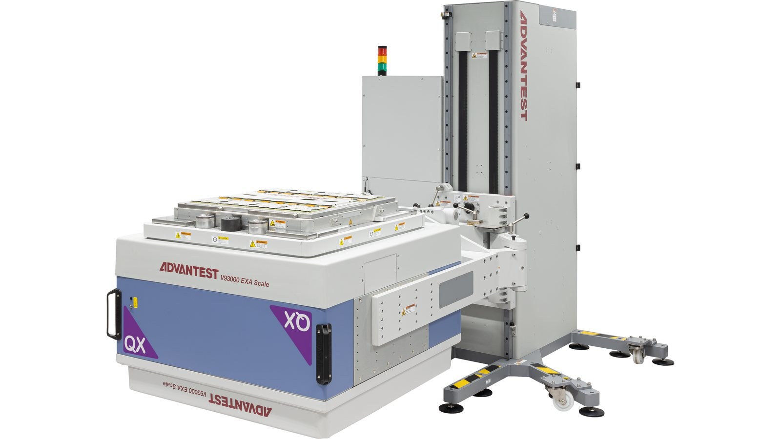
The V93000 EXA Scale QX test head extends Advantest’s scalable architecture to a four-card-cage design with 36 instrument slots · Foto: Advantest
Semiconductor Packaging

Advantest expands V93000 EXA Scale platform with new EXA Scale QX test head

Leading semiconductor test equipment supplier Advantest Corporation (TSE: 6857) has announced the V93000 EXA Scale QX test head, the latest addition to its EXA Scale SoC test platform. Designed to address the rapidly increasing test requirements of AI, high-performance computing (HPC) and advanced digital devices, the QX test head introduces a new four-card-cage, 36-slot architecture that provides unprecedented scalability for high-power and high-pin-count semiconductor devices.
Published
18 November 2026
Reading time
2 minutes
Section
Semiconductor Packaging

As AI and HPC devices continue to push the limits of power consumption, pin count and package complexity, semiconductor manufacturers require test infrastructure that can scale alongside evolving device architectures. The EXA Scale QX addresses these challenges by expanding the proven V93000 EXA Scale platform with additional slot capacity, power capability and digital density, enabling customers to support next-generation devices and emerging AI and HPC workloads while preserving continuity across their existing test environments.

Representing the next step in the EXA Scale platform’s evolution, the QX test head extends Advantest’s scalable architecture from CX (one card cage), SX (two card cages) and LX (three card cages) configurations to the new four-card-cage design. The EXA Scale QX test head maintains the established EXA Scale instrument and platform compatibility while expanding capacity to 36 instrument slots. With test head dimensions nearly identical to those of the EXA Scale LX, the EXA Scale QX maintains unrestricted compatibility with external equipment such as wafer probers, final test handlers and die-level probers. When integrated with the XHC32 double current pogo cable and XHD (Xtreme High Density) pogo blocks, the QX design provides an enhanced infrastructure that doubles the number of channels and amount of current per pogo block, enabling significantly higher overall power delivery while maintaining architectural continuity across card cages, backplanes, and system control.

Key power components are accommodated through an external rack, allowing the platform to scale without disrupting compatibility with the established EXA Scale ecosystem. With these features, the system supports demanding applications that require high current delivery, higher digital I/O counts, large reticle sizes, multi-site test, and greater test-head capacity — all within a trusted unified test platform.

“With EXA Scale QX, we are extending the V93000 single scalable platform to meet the most demanding future test requirements,” said Ralf Stoffels, Division Manager, V93000 Product Unit, Advantest. “As device architectures evolve toward higher power, higher pin counts, and advanced packaging, EXA Scale QX provides our customers with the infrastructure headroom they need, while preserving a consistent and scalable platform strategy.”

The EXA Scale QX is expected to be available in the first quarter of FY2027. Advantest will show the QX test head, along with its full line of automated test equipment and materials, at booth #W1779 at SEMICON Japan 2026 from 9 to 11 December at Tokyo Big Sight in Tokyo, Japan.

More from Semiconductor Packaging

More recent articles from Semiconductor Packaging.

All articles from Semiconductor Packaging
Nanoscribe scales photoresin manufacturing to industrial gradeFoto: Nanoscribe (semicon)
Semiconductor Packaging

Nanoscribe scales photoresin manufacturing to industrial grade

18 November 2026

Nanoscribe has invested in expanded manufacturing capabilities for five widely used photoresins, introducing industrial-grade quality standards and batch-specific CoA documentation to support growing adoption in optics…

Plasmatreat Presents Coordinated Plasma Portfolio for Semiconductor Surface Conditioning at SEMICON Europa 2026Foto: Plasmatreat (semicon)
Semiconductor Packaging

Plasmatreat Presents Coordinated Plasma Portfolio for Semiconductor Surface Conditioning at SEMICON Europa 2026

16 November 2026

At SEMICON Europa in Munich, Plasmatreat demonstrates how combining multiple plasma technologies enables controlled, reproducible surface conditions across advanced chip and packaging processes — from oxide reduction on…

Kosmek Publishes Semiconductor Manufacturing Automation CatalogFoto: Kosmek (semicon)
Semiconductor Packaging

Kosmek Publishes Semiconductor Manufacturing Automation Catalog

13 November 2026

Kosmek has released an industrial automation catalog focused on semiconductor manufacturing, detailing pneumatic supports, robotic hand changers and locating components applicable across front-end and back-end…

Nanoscribe Expands Photoresin Portfolio for Micro-Optics Fabrication via Two-Photon PolymerizationFoto: Brecht Corbeel / Unsplash
Semiconductor Packaging

Nanoscribe Expands Photoresin Portfolio for Micro-Optics Fabrication via Two-Photon Polymerization

11 November 2026

Nanoscribe has detailed its range of photoresins engineered for Two-Photon Polymerization (2PP) and Two-Photon Grayscale Lithography (2GL), targeting high-precision micro-optics manufacturing on silicon, glass, and…

← Zurück zu Semiconductor PackagingTo the homepage