Zum Inhalt springen
EPP Europe
  • News
  • Products
  • Applications
  • Technology
  • Semiconductor
  • Inspection
  • Company News
  • Events
EPP Europe
  • Technology
  • Inspection (AOI/AXI)
  • Semiconductor Packaging
  • Company News
  • Products
  • Trade Shows & Events
    EPP Europe Newsletter
    The most important electronics-manufacturing news delivered to your inbox.

    Info

    • Impressum
    • Datenschutz
    • Barrierefreiheit
    • Datenschutzeinstellungen

    Kontakt zur Redaktion

    EPP EuropeKonradin Mediengruppe
    Ernst-Mey-Str. 8, 70771 Leinfelden-Echterdingen

    E-Mail: redaktion@konradin.de
    Folgen Sie uns
    EPP Europe
    © 2026 EPP Europe
    Startseite/Technology/Artikel
    Nano Dimension offers 3D printed electronics with AME methodology
    Bildquelle nicht angegeben
    Technology

    Nano Dimension offers 3D printed electronics with AME methodology

    Nano Dimension's 3D printing solutions provide insights into how AME technology can drive electronics’ design forward.
    Veröffentlicht
    14. Januar 2021
    Lesezeit
    2 Minuten
    Rubrik
    Technology

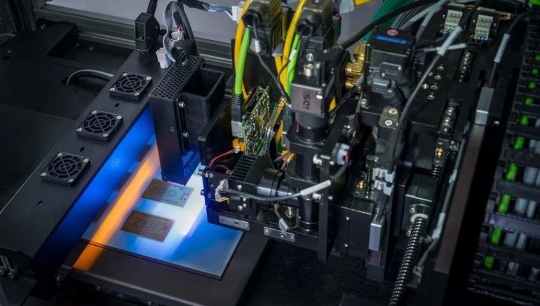
    Nano Dimension Ltd., a provider of Additively Manufactured Electronics (AME) and Printed Electronics (PE), offers quick solutions and easy access to complex PCBs and 3D printed electronics. Its unique and novel technology allows for rapid prototyping and production of high-performance electronic devices (Hi-PEDs).

    The company offers two solutions:

    • DragonFly LDM 3D-printing system for Hi-PEDs catering to cross-industry needs by enabling in-house printing of free-form, complex, multiple layered boards.
    • A printing service dubbed, NaNoS, for entities that wish to explore 3D printing of their own designs while gaining access to Nano’s 3D printing and design experts.

    “Nano Dimension bridges the gap between PCB and semiconductor integrated circuits,” said Yoav Stern, CEO. “A revolution at the click of a button: From CAD to a functional high-performance AME device in hours, solely for the cost of the consumable materials. The DragonFly LDM should be in everyone’s design workshop for rapid prototyping and testing. AME technology provides the capability to design and create free-form, multilayer complex circuit boards, bringing companies one-step closer to Industry 4.0. With NaNoS, the AME fabrication service becomes the first point of contact and an effective and affordable exploration of AME technology’s capabilities. This is a wake-up call for entities that wish to explore adoption of 3D revolutionary design, manufacturing, and fabrication technology.”

    The DragonFly LDM system enables in-house 3D printing of highly complex, multilayered circuits containing embedded capacitors, antennas, coils, converters, and electro-mechanical components, in just hours. They are also utilized in cutting edge research institutes, such as CBN-IIT (Italy) and the University of Technology in Sydney (Australia). These institutes continuously expand the design envelope by breaking free from traditional 2D PCB design rules, resulting in miniaturized, performance enhanced 3D AME devices.

    With approximately 60 systems sold worldwide, Nano Dimension is also cooperating with customers and partners such as Hensoldt (Germany), L3Harris (USA), and others, to provide insights into how AME technology can drive forward electronics’ design.

    The company has initiated a webinar-series where scientists and engineers share findings and AME-based solutions in 3D-printed 5G antennas, advanced microwave devices, embedding, micro-electromechanical systems (MEMS) packaging and heterogeneous integration. This knowledge sharing series provides a platform for the free flow of information and an open dialogue between industry experts who are looking for innovative solutions.

    Company contact

    Nano Dimension Ltd.
    13798 NW 4th Street, Suite 315
    Sunrise, Florida 33325
    Tel.: +1 408 824 8242
    Website: www.nano-di.com

    Mehr aus Technology

    Weitere aktuelle Artikel aus der Rubrik Technology.

    Alle Technology-Artikel
    IPC-J-STD-002F mandates automatic flux doctor blade for solderability testingFoto: Louis Reed / Unsplash
    Technology

    IPC-J-STD-002F mandates automatic flux doctor blade for solderability testing

    10. November 2026

    The release of IPC-J-STD-002 Revision F introduces stricter, more precisely defined requirements for solderability testing, including a mandatory automatic flux doctor blade on solderability testers. Equipment lacking…

    Plasmatreat PFW10 and PFW20 Static Plasma Jets Target Sensitive PCB Surface TreatmentFoto: Johannes Plenio / Unsplash
    Technology

    Plasmatreat PFW10 and PFW20 Static Plasma Jets Target Sensitive PCB Surface Treatment

    28. Oktober 2026

    Plasmatreat's PFW10 and PFW20 static plasma jet systems are designed for selective, high-accuracy surface treatment of sensitive electronic assemblies, including circuit boards, using cold atmospheric-pressure plasma.

    Indium Corporation to Present High-Reliability Solder Pastes at EFX 2026 in StuttgartFoto: Indium Corporation
    Technology

    Indium Corporation to Present High-Reliability Solder Pastes at EFX 2026 in Stuttgart

    30. September 2026

    Indium Corporation will exhibit three solder paste technologies at Expo for Electronics Manufacturing (EFX) 2026 in Stuttgart, Germany, addressing thermal cycling performance, low-temperature step soldering and…

    Europlacer: Software as the Core Performance Driver in High-Mix SMTFoto: Brecht Corbeel / Unsplash
    Technology

    Europlacer: Software as the Core Performance Driver in High-Mix SMT

    24. September 2026

    Europlacer makes the case that traditional SMT software was not designed for the demands of high-mix, short-run production, and that the resulting performance gap is increasingly visible on the shop floor.

    ← Zurück zu TechnologyZur Startseite