
Zum Inhalt springen
EPP Europe
  • News
  • Products
  • Applications
  • Technology
  • Semiconductor
  • Inspection
  • Company News
  • Events
EPP Europe
  • Technology
  • Inspection (AOI/AXI)
  • Semiconductor Packaging
  • Company News
  • Products
  • Trade Shows & Events
    EPP Europe Newsletter
    The most important electronics-manufacturing news delivered to your inbox.

    Info

    • Impressum
    • Datenschutz
    • Barrierefreiheit
    • Datenschutzeinstellungen

    Kontakt zur Redaktion

    EPP EuropeKonradin Mediengruppe
    Ernst-Mey-Str. 8, 70771 Leinfelden-Echterdingen

    E-Mail: redaktion@konradin.de
    Folgen Sie uns
    EPP Europe
    © 2026 EPP Europe
    Startseite/Semiconductor-packaging/Artikel
    Kulicke & Soffa Receives 2026 SEMI Award for Fluxless Thermocompression Bonding Technology
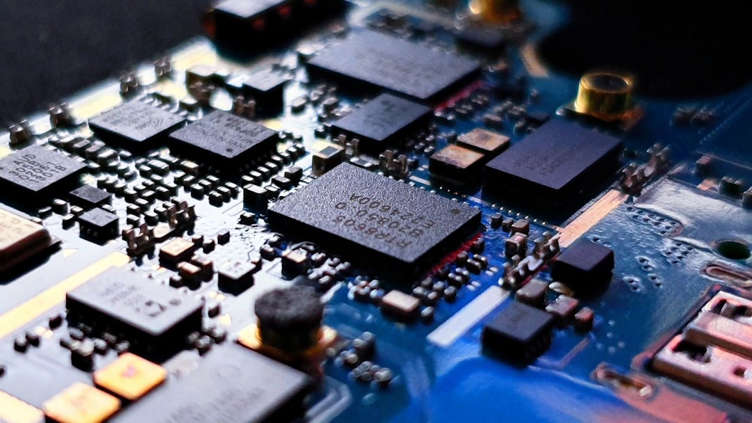
    Foto: ThisisEngineering / Unsplash
    Semiconductor-packaging

    Kulicke & Soffa Receives 2026 SEMI Award for Fluxless Thermocompression Bonding Technology

    Formic acid in situ bonding approach enables sub-10-micron interconnect pitches for heterogeneous integration
    Veröffentlicht
    14. Oktober 2026
    Lesezeit
    2 Minuten
    Rubrik
    Semiconductor-packaging

    SEMI, the industry association for the global semiconductor and electronics manufacturing supply chain, has named Kulicke & Soffa as the recipient of the 2026 SEMI Award for North America. The award was presented during the CEO Summit Keynotes at SEMICON West in San Francisco on 13 October 2026. The company was recognised for its formic acid in situ bonding technology, a fluxless thermocompression bonding (TCB) approach positioned as a cost-accessible alternative to hybrid bonding for heterogeneous integration applications.

    Conventional TCB processes face significant challenges at interconnect pitches of 50 microns and below, where post-bond liquid flux cleaning becomes increasingly difficult and time-consuming. Hybrid bonding addresses some of these limitations but introduces high process complexity and cost that restrict its applicability in volume manufacturing. Kulicke & Soffa's approach combines in situ formic acid oxide reduction with plasma pre-cleaning within its high-volume TCB platforms, aiming to deliver performance comparable to hybrid bonding at a materially lower cost basis.

    The technology is implemented in the company's APTURA platform, which integrates multiple oxide removal strategies in a single system. According to Kulicke & Soffa, this architecture enables interconnect pitches below 10 microns, addressing density requirements relevant to heterogeneous integration and silicon photonics packaging. The platform is designed to operate across wafer formats, supporting flexibility in production environments.

    Joe Stockunas, president of SEMI Americas, noted the relevance of the technology to AI and high-performance computing, sectors that are driving demand for increasingly dense interconnect solutions. He also highlighted that Kulicke & Soffa is a founding member of SEMI and is marking its 75th anniversary in 2026.

    From an advanced packaging perspective, fluxless TCB is gaining traction as chiplet-based architectures proliferate across logic, memory, and photonics applications. The ability to eliminate flux residues at fine pitches without resorting to the full process complexity of hybrid bonding is a practical consideration for contract manufacturers and IDMs scaling heterogeneous integration in volume. Kulicke & Soffa's APTURA platform enters a competitive field that includes equipment from ASM Pacific Technology and Besi, among others, making the SEMI recognition a notable marker of the technology's industry standing.

    Quelle: SEMICON Europa – https://www.semi.org/en/semi-press-release/kulicke-and-soffa-earns-2026-semi-award-for-north-america-at-semicon-west


    Mehr aus Semiconductor-packaging

    Weitere aktuelle Artikel aus der Rubrik Semiconductor-packaging.

    Alle Semiconductor-packaging-Artikel
    Nanoscribe Expands Photoresin Portfolio for Micro-Optics Fabrication via Two-Photon PolymerizationFoto: Brecht Corbeel / Unsplash
    Semiconductor-packaging

    Nanoscribe Expands Photoresin Portfolio for Micro-Optics Fabrication via Two-Photon Polymerization

    11. November 2026

    Nanoscribe has detailed its range of photoresins engineered for Two-Photon Polymerization (2PP) and Two-Photon Grayscale Lithography (2GL), targeting high-precision micro-optics manufacturing on silicon, glass, and…

    Canon Launches FPA-6400ES6a KrF Lithography System with 400 Wafers-per-Hour ThroughputFoto: Canon Europe (semicon)
    Semiconductor-packaging

    Canon Launches FPA-6400ES6a KrF Lithography System with 400 Wafers-per-Hour Throughput

    10. November 2026

    Canon has announced the FPA-6400ES6a KrF scanner for semiconductor lithography, combining a throughput of 400 wafers per hour with industry-leading overlay accuracy of 4.0 nm and the ability to handle wafer warpage of…

    Fabmatics absorbs SCI business activities under unified brandFoto: Ludovico Ceroseis / Unsplash
    Semiconductor-packaging

    Fabmatics absorbs SCI business activities under unified brand

    6. November 2026

    Fabmatics has integrated the business activities of SCI under the Fabmatics brand, consolidating the acquired expertise within its semiconductor automation portfolio.

    Entegris and Kioxia Expand Partnership on Materials Innovation for Next-Gen 3D Flash MemoryFoto: Louis Reed / Unsplash
    Semiconductor-packaging

    Entegris and Kioxia Expand Partnership on Materials Innovation for Next-Gen 3D Flash Memory

    6. November 2026

    Entegris and Kioxia are deepening their strategic partnership to co-develop materials and process technologies for future BiCS FLASH 3D NAND architectures, using AI, digital-twin modelling and experimental validation at…

    ← Zurück zu Semiconductor-packagingZur Startseite

