
Zum Inhalt springen
EPP Europe
  • News
  • Products
  • Applications
  • Technology
  • Semiconductor
  • Inspection
  • Company News
  • Events
EPP Europe
  • Technology
  • Inspection (AOI/AXI)
  • Semiconductor Packaging
  • Company News
  • Products
  • Trade Shows & Events
    EPP Europe Newsletter
    The most important electronics-manufacturing news delivered to your inbox.

    Info

    • Impressum
    • Datenschutz
    • Barrierefreiheit
    • Datenschutzeinstellungen

    Kontakt zur Redaktion

    EPP EuropeKonradin Mediengruppe
    Ernst-Mey-Str. 8, 70771 Leinfelden-Echterdingen

    E-Mail: redaktion@konradin.de
    Folgen Sie uns
    EPP Europe
    © 2026 EPP Europe
    Startseite/Semiconductor-packaging/Artikel
    Kulicke & Soffa Expands Thermal Compression Bonding Capabilities
    Bildquelle nicht angegeben
    Semiconductor-packaging

    Kulicke & Soffa Expands Thermal Compression Bonding Capabilities

    Kulicke & Soffa Expands Thermal Compression Bonding Capabilities to Accelerate Innovation in the Integration of Semiconductor and Silicon Photonics.
    Veröffentlicht
    11. März 2022
    Lesezeit
    2 Minuten
    Rubrik
    Semiconductor-packaging

    Kulicke and Soffa Industries, Inc., a global leader in the design and manufacture of semiconductor, LED and electronicassembly equipment, announced it is expanding its Thermal Compression Bonding (TCB) capabilities to accelerate innovation in the integration of semiconductor and Silicon Photonics.

    Multi-Chip integration is a fast-growing assembly trend supporting transistor-level density at the package level for both high-volume semiconductors and also leading-edge assembly. The Company’s broad assembly solutions are addressing current needs for Multi-Chip Module (MCM) assembly, System-in-Package (SiP) as well as the emerging market needs for Heterogeneous, or Chiplet, integration and also co-packaged optics. High-Performance Computing (HPC) and data center applications which support artificial intelligence, 5G, autonomous vehicles and wearable technology are demanding these emerging package types.

    During its first fiscal quarter of 2022, the Company successfully received acceptance and recognized revenue for a high-potential Silicon Photonics application which supports the emerging optical transceiver market. Optical transceivers represent a new market opportunity for K&S and are anticipated to grow at a 50% CAGR through 2025, supporting the growing need for increased global connectivity in data centers and HPC applications.

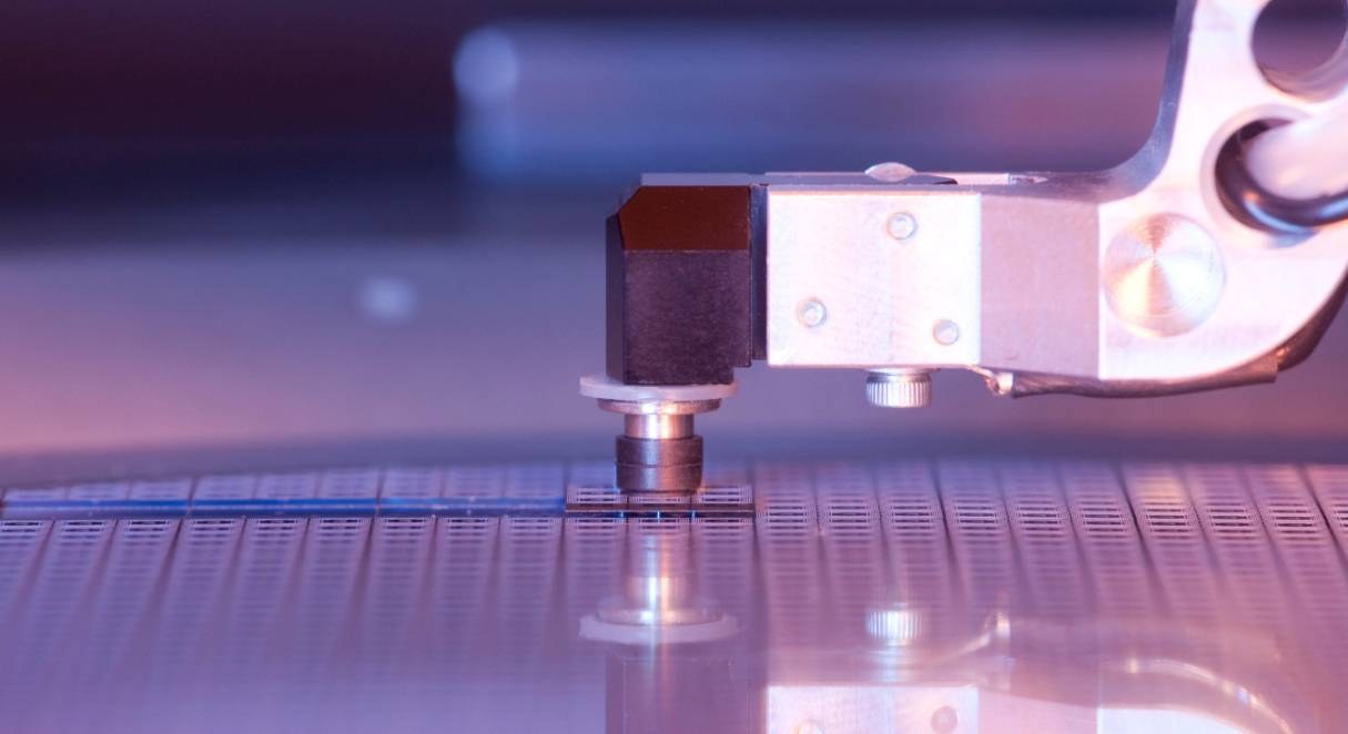
    Kulicke & Soffa’s TCB solution utilizes a unique formic acid process, that supports new assembly and packaging requirements for Silicon Photonics, the co-packaging of semiconductors and Silicon Photonics and 2.5D/3D heterogeneous integration.

    Chan Pin Chong, Kulicke & Soffa’s Executive Vice President of Products & Solutions, said, “A key challenge of multi-chip integration is the trade-off between performance and power consumption which our solutions are well positioned to optimize. We are privileged to be selected as the pioneer solution for co-packaged development utilizing thermal compression bonding, with formic acid, which directly addresses these critical process challenges and is expected to accelerate the adoption of emerging Silicon Photonics applications.”

    The Company will provide additional details regarding this opportunity during it’s upcoming earnings call scheduled for February 3, 2022 at 8am EST.

    About Kulicke & Soffa

    Kulicke & Soffa (NASDAQ: KLIC) is a leading provider of semiconductor, LED and electronic assembly solutions serving the global automotive, consumer, communications, computing and industrial markets. Founded in 1951,K&S prides itself on establishing foundations for technological advancement – creating pioneering interconnect solutions that enable performance improvements, power efficiency, form-factor reductions and assembly excellence of current and next-generation semiconductor devices. Leveraging decades of development proficiency and extensive process technology expertise, Kulicke & Soffa’s expanding portfolio provides equipment solutions, aftermarket products and services supporting a comprehensive set of interconnect technologies including wire bonding, advanced packaging, lithography, and electronics assembly. Dedicated to empowering technological discovery, always, K&S collaborates with customers and technology partners to push the boundaries of possibility, enabling a smarter future.


    Mehr aus Semiconductor-packaging

    Weitere aktuelle Artikel aus der Rubrik Semiconductor-packaging.

    Alle Semiconductor-packaging-Artikel
    Nanoscribe Expands Photoresin Portfolio for Micro-Optics Fabrication via Two-Photon PolymerizationFoto: Brecht Corbeel / Unsplash
    Semiconductor-packaging

    Nanoscribe Expands Photoresin Portfolio for Micro-Optics Fabrication via Two-Photon Polymerization

    11. November 2026

    Nanoscribe has detailed its range of photoresins engineered for Two-Photon Polymerization (2PP) and Two-Photon Grayscale Lithography (2GL), targeting high-precision micro-optics manufacturing on silicon, glass, and…

    Canon Launches FPA-6400ES6a KrF Lithography System with 400 Wafers-per-Hour ThroughputFoto: Canon Europe (semicon)
    Semiconductor-packaging

    Canon Launches FPA-6400ES6a KrF Lithography System with 400 Wafers-per-Hour Throughput

    10. November 2026

    Canon has announced the FPA-6400ES6a KrF scanner for semiconductor lithography, combining a throughput of 400 wafers per hour with industry-leading overlay accuracy of 4.0 nm and the ability to handle wafer warpage of…

    Fabmatics absorbs SCI business activities under unified brandFoto: Ludovico Ceroseis / Unsplash
    Semiconductor-packaging

    Fabmatics absorbs SCI business activities under unified brand

    6. November 2026

    Fabmatics has integrated the business activities of SCI under the Fabmatics brand, consolidating the acquired expertise within its semiconductor automation portfolio.

    Entegris and Kioxia Expand Partnership on Materials Innovation for Next-Gen 3D Flash MemoryFoto: Louis Reed / Unsplash
    Semiconductor-packaging

    Entegris and Kioxia Expand Partnership on Materials Innovation for Next-Gen 3D Flash Memory

    6. November 2026

    Entegris and Kioxia are deepening their strategic partnership to co-develop materials and process technologies for future BiCS FLASH 3D NAND architectures, using AI, digital-twin modelling and experimental validation at…

    ← Zurück zu Semiconductor-packagingZur Startseite

