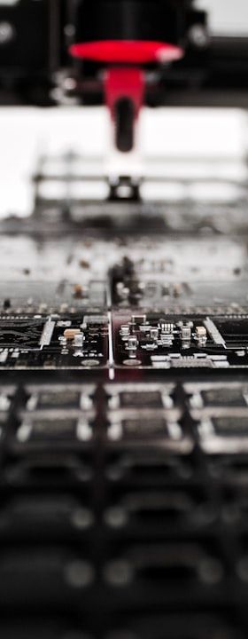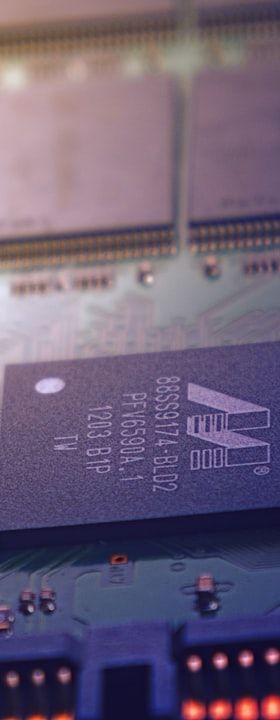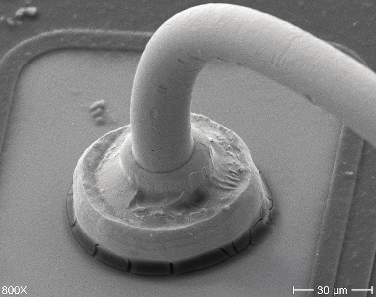
Small electrical parts can cause a lot of damage. These parts can now be found in nearly every device, and not only are the amounts of parts increasing, but also at the same time miniaturizing, which raises the amount of potential failures in a device. Currently, applied packaging concepts on chip-to-chip or chip-to-wafer level are used commercially in products, such as smart phones, cameras, and laptops. Due to the increasing needs of electronic system manufacturers, an optimal combination of functionality, performance, reliability and price is requested. The geometric dimensions of the systems also play a decisive role.
For example, the dense construction on a board used in a smart- phone can lead to over 10.000 possible causes of malfunction– a risk for developers, as well as, decision makers, which could exceed the usual regulatory requirements of functionality and reliability. This development challenges external testing service providers – and engineers to choose state-of-the-art solutions in quality testing.
The causes of defects are diversified. Failures can lead to even bigger catastrophes, often combined with human failure or lack in quality. Especially in the process chain, where one part comes from another country or even continent, it is smarter for OEMs and designing engineers to think before taking action (by means of serial production).
Part of a damage investigation is to develop solutions and improvements for the production process, together with clients. The overall aim is to avoid future failures and to reduce the resulting warranty and maintenance costs. Today, damage analysis experience within companies (suppliers as well as manufacturers/constructors) is mostly insufficient, consequently external suppliers with specific knowledge are becoming more and more significant. Technical equipment and extensive know-how allow the investigation of faulty or suspect objects to be carried out efficiently and with high security of evidence. In addition, specialists are able to secure a critical chain of evidence through damage simulation.
TechnoLab GmbH is a service provider in the field of environmental simulation and damage analysis, with headquarters in Berlin operating globally across a variety of industries. The company offers material tests, quality inspections, certifications in accordance with current standards and, if required, develops individual solutions beyond standard dimensions. Damage analyses help developers optimize and secure their manufacturing process.
Main focus is on electronic assemblies: their use and process chain
The environmental simulation tests check the resistance of materials, individual components, assemblies, as well as entire devices and can be customized to meet individual requirements. It tests for any chemical-biological, physical or other effects, such as IP protection, temperature change, often combined with altitude/vacuum, vibration & shock, salt compatibility or solar radiation. In fields, such as chemical and biological resistance, noxious gas as well as blowing-sand, the company has unique capacities in Germany and Europe with an enlarged blowing-sand, even with a dust chamber with up to 25.000 liters volume. Mobile devices are also testable with a simulated speed of over 300 km/h.