Peter van den Eijnden, JTAG Technologies, Eindhoven (NL)
However, because of the way boundary-scan works, it also has the potential to provide great assistance during prototype development and debug work; particularly when there is limited or no access to device pins/pads. Historically though, engineers have seldom been able to justify the purchase of a ‘manufacturing test tool’ for development work. Until now.
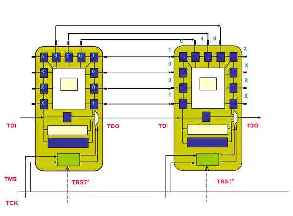
Boundary-scan works by ‘taking control’ of the pins/pads of boundary-scan compliant components on a PCB. Here, ‘compliant’ means that it is a boundary-scan version of a standard digital component but with at least three additional internal registers. These are the principal Boundary-Scan test Register (BSR), an Instruction Register and a Bypass Register. The device will also have four or five additional pins/pads that constitute its Test Access Port (TAP).
Excluding the TAP and power/ground pins/pads, the devices’ other digital pins/pads will usually each have a boundary-scan cell (or cells)connected internally. The cells will be transparent during normal operation but can be placed in a chain (or shift register) around the ‘inner perimeter’ of the device.
The three internal registers are accessed by the TAP – and data comes into the device on TDI (Test Data In) and exits on TDO (Test Data Out). TCK (Test Clock) and TMS (Test Mode Select) facilitate control and, if present, a TRST is for reset.
For a board with multiple boundary-scan devices present, TCK, TMS and TRST would be placed in parallel. TDI and TDO would be daisy-chained. All would terminate at a board TAP. Also, a PCB can have more than one boundary-scan chain if desired.
Following the build of a prototype board, a boundary-scan test controller can be used to inject a pattern of 1s and 0 s into the cells of the boundary-scan chain which are ‘lined up’ on the physical pins/pads of some of the devices. The pins/pads of other devices – connected by the PCB’s nets/tracks – can then be read by first capturing the data into the BSR and then clocking it out of the chain. Looking for the expected patterns is effectively buzzing out the board, as variations from the expected will be indicative of board and/or device problems.
Used in conjunction with traditional methods – such as a multimeter, scope or bed-of-nails tester, it is possible to look for certain logic states on non-boundary-scan devices or at edge connectors. Also, limited functional test is equally feasible. For example, a test pattern or patterns could be lined up on the edge of a boundary-scan device known to be connected to the input of a (non-boundary-scan) DAC in order to produce an analogue value.
Boundary-scan compliant devices cost little, if any, more than their non-boundary-scan counterparts; indeed many designs may already feature boundary-scan (IEEE std. 1149.1) compliant parts. Also, there is only a small overhead during schematic capture, as designing in boundary-scan devices requires the addition of only a few more nets.
As for control of the devices and performing tests, the boundary-scan software and controllers do the majority of the hard work by making use of boundary-scan description language (BSDL) files available from the device vendors.
So all in all, boundary-scan has huge potential within the development arena; and whilst costs to date have proved prohibitive, productronica 2009 saw the launch of the JTAG Live family of boundary-scan tools. It comprises three products, Buzz, Clip, and Script – each of which is targeted at different aspects of the debugging process.
Of these, Buzz is available free-of-charge from the website and provides the ability to check quickly (direct and indirect) connections between devices supporting boundary-scan. This is effectively a practical way to check continuity between two pins on a prototype board – mimicking the familiar DMM ‘buzz’ measurement but without probes. Also, the site includes product descriptions, answers to FAQs, and highlighted experiences from JTAG Live users. The Clip and Script tools (equally invaluable for development/debug work) are also available for download but for a charge.
A ‘Watch’ window in Buzz shows the current logic state (High, Low or Toggling) of any selected boundary-scan pin and continuity checks can be performed through a Measure window; which allows device pins to be driven High or Low and other pins configured to sense. This goes beyond the functionality of a traditional DMM, as multi-pin nets can be tested simultaneously. For example, it is possible to drive one pin to many to check for correct fan-out connectivity or to drive from multiple pins to one or more sense pins to perform a test on bus lines (or to verify a simple cluster comprising one or more logic gates).
To connect to the board, JTAG Live is fully compatible with the popular JTAG programming cables from Altera and Xilinx, as well as a two-port JT3705/USB Explorer from the company.
Free, JTAG Live Buzz is the perfect introduction to boundary-scan testing for designers making their first forays into the realms of design for test. The structured and modular approach to the system also allows users to expand their capabilities progressively and at a modest cost.
productronica, A1.458
In diesem Artikel wird erläutert, wie optimal sich der Einsatz eines kostenlosen Boundary-Scan-Test-Tools bei der Fehlersuche im Prototyping auswirken kann, und wie es angewendet wird. Der Vorteil, es steht kostenlos zum Download zur Verfügung.
Dans cet article, on explique l’efficacité que peut atteindre l’utilisation d’un Boundary-Scan-Test-Tool gratuit dans la recherche d’erreurs dans le domaine des prototypes et comment cet outil est appliqué. L’avantage : il est en téléchargement gratuit.