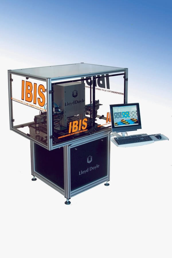
It uses massively parallel digital signal processing technology coupled with true white light interferometry to offer 20 to 30 times improvement over existing interferometry systems previously available. The company’s proprietary enhancements give IBIS the edge for solder bump height measurement. This enabling technology will be transportable to wafer and chip solder bump measurement in the future.
“This system represents a breakthrough in inspecting and measuring bump parameters accurately at high speed,” said Roy Lloyd, CEO. “It will enable manufacturers to have 100 percent inspection of solder bumps on chip carriers rather than only being able to measure these under laboratory conditions.”
EPP Europe 438