
Zum Inhalt springen
EPP Europe
  • News
  • Products
  • Applications
  • Technology
  • Semiconductor
  • Inspection
  • Company News
  • Events
EPP Europe
  • Technology
  • Inspection (AOI/AXI)
  • Semiconductor Packaging
  • Company News
  • Products
  • Trade Shows & Events
    EPP Europe Newsletter
    The most important electronics-manufacturing news delivered to your inbox.

    Info

    • Impressum
    • Datenschutz
    • Barrierefreiheit
    • Datenschutzeinstellungen

    Kontakt zur Redaktion

    EPP EuropeKonradin Mediengruppe
    Ernst-Mey-Str. 8, 70771 Leinfelden-Echterdingen

    E-Mail: redaktion@konradin.de
    Folgen Sie uns
    EPP Europe
    © 2026 EPP Europe
    Startseite/Semiconductor-packaging/Artikel
    Indium Corporation to Present Advanced Packaging Materials Research at CPRIM 2026
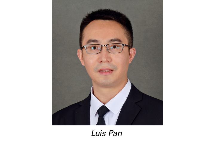
    Foto: Indium Corporation
    Semiconductor-packaging

    Indium Corporation to Present Advanced Packaging Materials Research at CPRIM 2026

    Senior Technical Manager Luis Pan to address co-innovation of interconnect materials and assembly processes for improved yield and reliability in semiconductor packaging
    Veröffentlicht
    03. September 2026
    Lesezeit
    2 Minuten
    Rubrik
    Semiconductor-packaging

    Indium Corporation will present at CPRIM 2026 on September 4 in Guangzhou, China. Senior Area Technical Manager Luis Pan will deliver a presentation titled 'Co-innovation of Materials and Processes for Advanced Semiconductor Packaging', focusing on how the selection and development of interconnect materials directly influence process outcomes in advanced packaging applications.

    The presentation covers several specific material and process topics that are increasingly relevant to high-density semiconductor packaging. These include heat-stable fluxes designed for thermocompression bonding (TCB) and laser-assisted bonding (LAB) processes, both of which impose elevated thermal loads on flux chemistry compared with conventional reflow. Pan will also address ultra-low residue flux formulations developed for compatibility with underfill materials — a critical consideration where residue incompatibility can compromise adhesion, void formation, or underfill flow characteristics.

    Additional topics include Indium Corporation's SiPaste technology, positioned for fine-pitch, high-density interconnect applications, and near-zero-residue bonding materials intended for fluxless assembly environments. Fluxless or near-fluxless assembly is of growing interest in wafer-level and chip-scale packaging where residue removal is impractical or where contamination of sensitive structures must be minimised.

    The presentation speaks to a broader industry challenge: as semiconductor packaging architectures become more complex — encompassing heterogeneous integration, chiplet-based designs, and 2.5D/3D stacking — the interdependence between material formulation and process parameters becomes more consequential. Flux activation windows, residue volume, thermal stability, and compatibility with subsequent process steps such as underfilling or encapsulation all require coordinated development rather than independent optimisation.

    Luis Pan manages the regional technical support team in South China and is based at Indium Corporation's Shenzhen facility. He brings 20 years of industry experience spanning SMT equipment, assembly processes, product design, and new product introduction. Pan holds a bachelor's degree in automation from Southwest University of Science and Technology and holds certifications as a project management professional and ISO 9001 internal auditor.

    CPRIM 2026 is scheduled for September 4, with Pan's session taking place at 15:00–15:20 China Standard Time. Indium Corporation's broader packaging materials portfolio, including solders, fluxes, brazes, and thermal interface materials, is documented at indium.com.

    Quelle: Indium Corporation – https://www.indium.com/press-releases/indium-corporation-to-explore-the-critical-materials-and-packaging-process-connection-at-cprim-2026/


    Mehr aus Semiconductor-packaging

    Weitere aktuelle Artikel aus der Rubrik Semiconductor-packaging.

    Alle Semiconductor-packaging-Artikel
    Nanoscribe Expands Photoresin Portfolio for Micro-Optics Fabrication via Two-Photon PolymerizationFoto: Brecht Corbeel / Unsplash
    Semiconductor-packaging

    Nanoscribe Expands Photoresin Portfolio for Micro-Optics Fabrication via Two-Photon Polymerization

    11. November 2026

    Nanoscribe has detailed its range of photoresins engineered for Two-Photon Polymerization (2PP) and Two-Photon Grayscale Lithography (2GL), targeting high-precision micro-optics manufacturing on silicon, glass, and…

    Canon Launches FPA-6400ES6a KrF Lithography System with 400 Wafers-per-Hour ThroughputFoto: Canon Europe (semicon)
    Semiconductor-packaging

    Canon Launches FPA-6400ES6a KrF Lithography System with 400 Wafers-per-Hour Throughput

    10. November 2026

    Canon has announced the FPA-6400ES6a KrF scanner for semiconductor lithography, combining a throughput of 400 wafers per hour with industry-leading overlay accuracy of 4.0 nm and the ability to handle wafer warpage of…

    Fabmatics absorbs SCI business activities under unified brandFoto: Ludovico Ceroseis / Unsplash
    Semiconductor-packaging

    Fabmatics absorbs SCI business activities under unified brand

    6. November 2026

    Fabmatics has integrated the business activities of SCI under the Fabmatics brand, consolidating the acquired expertise within its semiconductor automation portfolio.

    Entegris and Kioxia Expand Partnership on Materials Innovation for Next-Gen 3D Flash MemoryFoto: Louis Reed / Unsplash
    Semiconductor-packaging

    Entegris and Kioxia Expand Partnership on Materials Innovation for Next-Gen 3D Flash Memory

    6. November 2026

    Entegris and Kioxia are deepening their strategic partnership to co-develop materials and process technologies for future BiCS FLASH 3D NAND architectures, using AI, digital-twin modelling and experimental validation at…

    ← Zurück zu Semiconductor-packagingZur Startseite

