
Indium Corporation will present its power device packaging materials portfolio at PCIM Asia 2026, scheduled for 26–28 August in Shenzhen, China. The Clinton, N.Y.-based company, which operates as a materials refiner, smelter, and supplier to the global electronics and semiconductor industries, is exhibiting at Hall 16, Booth F30.
Central to the showcase is the company's Formic Acid Soldering Technology (FAST), a flux-free reflow method suited to power device packaging environments where residue management and voiding control are critical. Associated product forms include solder preforms, InFORMS flexible solder preforms, and dedicated solder pastes. Flux-free processing is increasingly relevant for hermetic and high-density power module assemblies where post-solder cleaning is impractical or where ionic contamination presents reliability risks.
In the sintering materials segment, Indium Corporation is presenting its InFORCE range of pressure sinter pastes in both silver and copper formulations. The product line is characterised by high metal content and low organic loading, which the company states results in shorter drying cycles and reduced volume shrinkage between wet deposit and post-sintered state — factors directly relevant to yield and throughput in automated dispensing or printing processes.
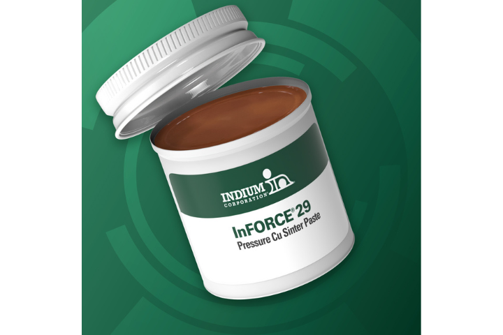
InFORCE 29 is a copper-based pressure sinter paste targeting die-attach for silicon and silicon carbide power devices, as well as substrate-to-cooler attach in power modules. Copper sintering has attracted substantial industry interest as an alternative to silver sintering, particularly in cost-sensitive or high-volume applications, given the relative material cost and electromigration characteristics of the two metals.
InFORCE MF is a silver-based pressure sinter paste formulated specifically for SiC die-attach. According to Indium Corporation, it is compatible with both printing and dry-placement processes and is characterised by high die shear strength and thermal conductivity — properties critical in SiC-based inverter and converter modules operating at elevated junction temperatures.
Complementing the pressure-sinter range, InBAKE 29 is a copper sinter paste developed for pressureless, batch oven sintering. This approach removes the need for pressure tooling during the sintering step, which can simplify process equipment requirements for manufacturers handling complex or large-format substrates. Target applications include power discrete die-attach where high thermal conductivity, high electrical conductivity, and elevated service temperatures are required.
From a European electronics manufacturing perspective, the demand for advanced die-attach and substrate-attach materials is being driven by the ongoing electrification of automotive powertrains, industrial motor drives, and renewable energy conversion systems. SiC device adoption is accelerating across these sectors, and the associated packaging requirements — particularly regarding thermal interface performance and long-term thermomechanical reliability — are pushing process engineers toward sintered interconnects as an alternative to conventional solder-based die-attach. Materials suppliers such as Indium Corporation are responding with broader product portfolios that address both silver and copper sintering routes, as well as flux-free soldering for applications where traditional paste-based processes are not appropriate.
Quelle: Indium Corporation – https://www.indium.com/press-releases/indium-corporation-to-showcase-high-reliability-power-device-packaging-solutions-at-pcim-asia-2026/



