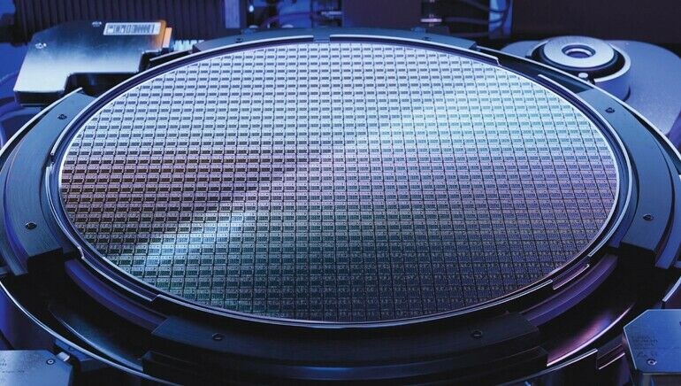
Wafer fabrication is a highly intricate, multi-step process where electronic circuits are progressively constructed on a semiconductor substrate. A single wafer can host hundreds to thousands of ICs, which are subsequently prepared for integration through bumping (for flip-chip soldering) or wire bonding, followed by die singulation and encapsulation via molding.
Due to the wafers‘ fragility, micron-level dimensions, and contamination risks, manual handling is impractical. Therefore, automation is leveraged at every stage of semiconductor manufacturing and testing, ensuring repeatability, high throughput, and minimal human intervention.
Automated Wafer Testing
Wafer testing, a crucial step in semiconductor production, employs a combination of electrical and optical inspection methodologies to assess device performance and identify defects. Automatic Test Equipment (ATE) interfaces with the wafer through a probe card, performing parametric and functional tests across analog, digital, and mixed-signal domains.
Each die undergoes electrical characterization to validate operational integrity. Defective dies are mapped out, while functional dies—classified as Known Good Die (KGD)—proceed to subsequent packaging and assembly stages. This testing phase generates wafer maps with detailed pass/fail status for each die, facilitating downstream process optimization.
Precision and Challenges in Wafer Testing
Wafer-level testing requires handling silicon substrates with extreme care. Modern silicon wafers have diameters ranging from 100 mm (4“) to 300 mm (12“) and thicknesses of approximately 400–500 µm. The individual circuit features on each die are measured at sub-micron levels, demanding precise probe alignment, controlled contact force, and advanced signal integrity considerations during testing.
Given these constraints, test engineers rely on sophisticated probing technologies, including MEMS-based probe cards and advanced probing systems, to achieve high pin-count, fine-pitch probing without damaging the delicate wafer structures.
By leveraging automation and precision testing methodologies, semiconductor manufacturers can optimize yields, reduce production costs, and enhance IC reliability before devices enter final packaging and system-level integration.
About Seica S.p.A.
Founded in 1986, Seica S.p.A. is an innovative, high technology company that develops and manufactures leading-edge solutions for the test and selective soldering of electronic boards and modules. Moreover, the company provides battery test solutions, automotive electronic board test solutions, infotainment test, as well as electric vehicle inverter and battery charging station test systems. The company has fully embraced the concept of Industry 4.0, developing solutions to monitor and collect information from machines and industrial plants to enable the optimization of manufacturing processes, maintenance and energy management. Headquarters are located in Italy, with direct offices in Germany, France, China, the USA, Mexico and Israel.