Zum Inhalt springen
EPP Europe
  • News
  • Products
  • Applications
  • Technology
  • Semiconductor
  • Inspection
  • Company News
  • Events
EPP Europe
  • Technology
  • Inspection (AOI/AXI)
  • Semiconductor Packaging
  • Company News
  • Products
  • Trade Shows & Events
    EPP Europe Newsletter
    The most important electronics-manufacturing news delivered to your inbox.

    Info

    • Impressum
    • Datenschutz
    • Barrierefreiheit
    • Datenschutzeinstellungen

    Kontakt zur Redaktion

    EPP EuropeKonradin Mediengruppe
    Ernst-Mey-Str. 8, 70771 Leinfelden-Echterdingen

    E-Mail: redaktion@konradin.de
    Folgen Sie uns
    EPP Europe
    © 2026 EPP Europe
    Startseite/Applications/Artikel
    Higher yield 300 mm wafer singulation
    Bildquelle nicht angegeben
    Applications

    Higher yield 300 mm wafer singulation

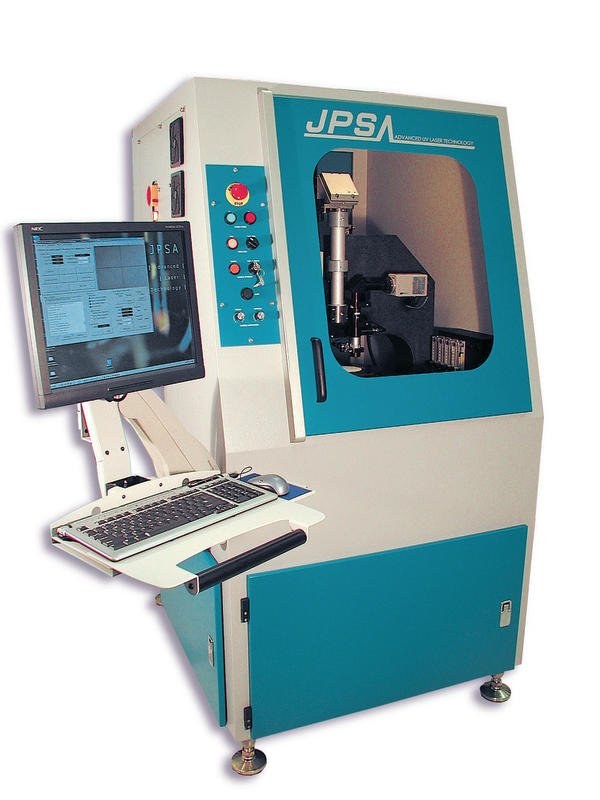
    The patented Chroma-Dice UV-DPSS laser systems from J. P. Sercel Associates can now scribe and dice 300 mm silicon wafers up to 500 microns thick. These
    Veröffentlicht
    12. April 2007
    Lesezeit
    2 Minuten
    Rubrik
    Applications

    The company’s Chroma-Dice systems feature high-performance, ultra-precise air bearing stages that provide higher speed and acceleration in addition to greater travel for wafers up to 300 mm. The system is also available with either 355 nm or 266 nm high-power, short pulse UV lasers for high speed, high yield processing of a range of materials as well as sapphire, silicon, and GaAs wafers.

    The systems are available with complete wafer handling systems including cassette loading. An upgraded laser diode wafer edge detector is available for all wafer types. This module interfaces with the new motion control system and allows any type of wafer, as well as partial wafers, to be processed on standard dicing tape frames with no damage to the dicing tape, thus allowing breaking and stretching for pick and place die transfer.

    According to the company with this larger wafer handling capability, customers can achieve increased process efficiency, even on thicker wafers. Since the heat-affected zones are minimised, cuts are clean and stress-free, so die count per wafer is higher than with traditional scribing methods, and economic payback is improved thanks to yields in excess of 99 %.

    The products and services include UV excimer and DPSS laser micromachining systems, UV and VUV laser beam delivery systems, UV laser materials processing development, optical damage testing, and excimer laser refurbishment services.

    www.jpsalaser.com

    EPP EUROPE 467

    Mehr aus Applications

    Weitere aktuelle Artikel aus der Rubrik Applications.

    Alle Applications-Artikel
    Expert to highlight new solder paste in Rosemont
    Applications

    Expert to highlight new solder paste in Rosemont

    25. August 2025

    AIM Solder is participating in the upcoming SMTA International 2025 event, which is taking place from October 19–23 at the Donald E. Stephens Convention

    Selective soldering machine take production to a new level
    Applications

    Selective soldering machine take production to a new level

    27. Mai 2025

    Under the motto “Assembling the Future”, Phonotronica Ltd. has been a pioneer in the development and manufacture of electronic modules since 1990.

    ← Zurück zu ApplicationsZur Startseite