Zum Inhalt springen
EPP Europe
  • News
  • Products
  • Applications
  • Technology
  • Semiconductor
  • Inspection
  • Company News
  • Events
EPP Europe
  • Technology
  • Inspection (AOI/AXI)
  • Semiconductor Packaging
  • Company News
  • Products
  • Trade Shows & Events
    EPP Europe Newsletter
    The most important electronics-manufacturing news delivered to your inbox.

    Info

    • Impressum
    • Datenschutz
    • Barrierefreiheit
    • Datenschutzeinstellungen

    Kontakt zur Redaktion

    EPP EuropeKonradin Mediengruppe
    Ernst-Mey-Str. 8, 70771 Leinfelden-Echterdingen

    E-Mail: redaktion@konradin.de
    Folgen Sie uns
    EPP Europe
    © 2026 EPP Europe
    Startseite/Applications/Artikel
    High-resolution 3D surface profile measurements made easy
    Bildquelle nicht angegeben
    Applications

    High-resolution 3D surface profile measurements made easy

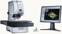
    Olympus’ Lext is a confocal laser-scanning microscope for ultra-precise measurement and observation. No sample preparation is required as they can be
    Veröffentlicht
    26. August 2005
    Lesezeit
    2 Minuten
    Rubrik
    Applications

    Lext is claimed setting standards in usability and measuring speed by a special operation concept. A 2-channel live display provides the opportunity to show a conventional colored microscope image and a confocal image in parallel. After the scan area had been defined by focusing on the top and on the bottom surface of the specimen, the scan process is running automatically. To allow the scan of surfaces with different reflection characteristics, such as the substrates and copper surface of a PCB, the instrument features an enhanced mode delivering clear images. All measurement functions are available, such as to analyze the shape of the surface, the height, distance, angle and volume. Lext allows measuring of roughness not only on one line but also on an area. Interpretation of results is getting much easier as the surface can be displayed in three dimensions, and surface, waviness and roughness can be separated. An optional motorized scanning stage enables automated image acquisition and measuring on several points of a specimen. Defects of metal corrosion that cannot be shown by monochrome pics are displayed in 3D color images, enabling more comprehensive analysis than is possible by SEM (scanning electron microscopy).

    www.olympus-europa.com

    EPP EUROPE 439

    Mehr aus Applications

    Weitere aktuelle Artikel aus der Rubrik Applications.

    Alle Applications-Artikel
    Expert to highlight new solder paste in Rosemont
    Applications

    Expert to highlight new solder paste in Rosemont

    25. August 2025

    AIM Solder is participating in the upcoming SMTA International 2025 event, which is taking place from October 19–23 at the Donald E. Stephens Convention

    Selective soldering machine take production to a new level
    Applications

    Selective soldering machine take production to a new level

    27. Mai 2025

    Under the motto “Assembling the Future”, Phonotronica Ltd. has been a pioneer in the development and manufacture of electronic modules since 1990.

    ← Zurück zu ApplicationsZur Startseite