Zum Inhalt springen
EPP Europe
  • News
  • Products
  • Applications
  • Technology
  • Semiconductor
  • Inspection
  • Company News
  • Events
EPP Europe
  • Technology
  • Inspection (AOI/AXI)
  • Semiconductor Packaging
  • Company News
  • Products
  • Trade Shows & Events
    EPP Europe Newsletter
    The most important electronics-manufacturing news delivered to your inbox.

    Info

    • Impressum
    • Datenschutz
    • Barrierefreiheit
    • Datenschutzeinstellungen

    Kontakt zur Redaktion

    EPP EuropeKonradin Mediengruppe
    Ernst-Mey-Str. 8, 70771 Leinfelden-Echterdingen

    E-Mail: redaktion@konradin.de
    Folgen Sie uns
    EPP Europe
    © 2026 EPP Europe
    Startseite/Products/Artikel
    Hensoldt and Nano Dimension create multi-layer PCB with 3D printing
    Bildquelle nicht angegeben
    Products

    Hensoldt and Nano Dimension create multi-layer PCB with 3D printing

    Nano Dimension and Hensoldt have achieved a major breakthrough on its way to utilizing 3D printing and assembled a multi-layer PCB.
    Veröffentlicht
    28. Mai 2020
    Lesezeit
    2 Minuten
    Rubrik
    Products

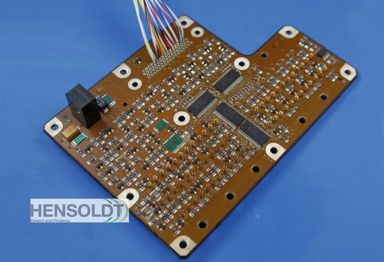
    Sensor solutions provider Hensoldt together with the Additively Manufactured Electronics (AME)/Printed Electronics (PE) provider, Nano Dimension, has achieved a major breakthrough on its way to utilizing 3D printing in the development process of high-performance electronics components. Utilizing a newly developed dielectric polymer ink and conductive ink from Nano Dimension, Hensoldt succeeded in assembling a 10-layer printed circuit board (PCB), which carries high-performance electronic structures soldered to both outer sides. Until now, 3D printed boards could not bear the soldering process necessary for two-sided population of components.

    “Military sensor solutions require performance and reliability levels far above those of commercial components.” says Hensoldt CEO, Thomas Müller. “To have high-density components quickly available with reduced effort by means of 3D printing gives us a competitive edge in the development process of such high-end electronic systems.”

    “Nano Dimension’s relationship with Hensoldt is the type of partnership with customers we are striving for,” commented Yoav Stern, Nano Dimension President & CEO. “Working together and learning from Hensoldt led us to reach a first-of-its-kind in-depth knowledge of polymer materials applications. Additionally, it guided us in the development of Hi-PEDs (High Performance Electronic Device) that create competitive edges by enabling unique implementations with shortest time to market.”

    AMEs are useful to verify a new design and functionality of specialized electronic components before production. It is a highly agile and individual engineering methodology to prototype a new electronic circuitry. This leads to significant reduction of time and cost in the development process. Furthermore, AME allows for a verified and approved design before production starts, leading to higher quality of the final product.

    The collaboration first started in 2016, in order to examine the possibilities of 3D printing electronics. Last year, Hensoldt successfully implemented the Nano Dimension’s DragonFly Lights-Out Digital Manufacturing (LDM) printing technology, an additive manufacturing platform for round-the-clock 3D printing of electronic circuitry.

    Nano Dimension
    2 Ilan Ramon St.
    Ness-Ziona Science Park
    Ness Ziona 7403635, Israel
    Website: www.nano-di.com
    Mehr aus Products

    Weitere aktuelle Artikel aus der Rubrik Products.

    Alle Products-Artikel
    Heavy board options added to reflow soldering system
    Products

    Heavy board options added to reflow soldering system

    27. Mai 2025

    Provider of reflow soldering technology, Vitronics Soltec has launched new Heavy Board options for its Centurion 1240 reflow soldering system. This

    New 3D AXI platform provides clearer imaging
    Products

    New 3D AXI platform provides clearer imaging

    22. Januar 2025

    Test Research, Inc. (TRI) has announced the launch of its new 3D AXI TR7600FB SII system and emphasized that it has been designed to deliver clearer

    No-clean formula maximize the solderability
    Products

    No-clean formula maximize the solderability

    10. Januar 2025

    Indium Corporation announced the global availability of CW-807RS, a new high-reliability, halide- and halogen-free flux-cored wire that improves wetting

    Extensive program of testing options
    Products

    Extensive program of testing options

    10. Januar 2025

    Test Research, Inc. (TRI) will join the IPC APEX EXPO 2025 held at Anaheim Convention Center on March 18 – 20, 2025 at booth #2905 to show latest test and

    ← Zurück zu ProductsZur Startseite