Zum Inhalt springen
EPP Europe
  • News
  • Products
  • Applications
  • Technology
  • Semiconductor
  • Inspection
  • Company News
  • Events
EPP Europe
  • Technology
  • Inspection (AOI/AXI)
  • Semiconductor Packaging
  • Company News
  • Products
  • Trade Shows & Events
    EPP Europe Newsletter
    The most important electronics-manufacturing news delivered to your inbox.

    Info

    • Impressum
    • Datenschutz
    • Barrierefreiheit
    • Datenschutzeinstellungen

    Kontakt zur Redaktion

    EPP EuropeKonradin Mediengruppe
    Ernst-Mey-Str. 8, 70771 Leinfelden-Echterdingen

    E-Mail: redaktion@konradin.de
    Folgen Sie uns
    EPP Europe
    © 2026 EPP Europe
    Startseite/Products/Artikel
    Flying probe tester for substrates
    Bildquelle nicht angegeben
    Products

    Flying probe tester for substrates

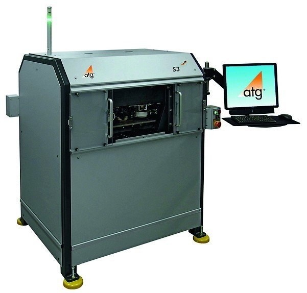
    atg Luther & Maelzer has delivered the first flying probe system for substrate test. The S3 10 µm Substrate Tester is the first system of a new
    Veröffentlicht
    15. Juli 2016
    Lesezeit
    1 Minute
    Rubrik
    Products

    Substrates are used to enable a connection between a semiconductor and a printed circuit board. A characteristic test panels consists of about 50 – 100 single substrates and has a size of approx. 250 mm x 80 mm. For electrical testing it is necessary to contact all end points of the product. Each substrate has about 1000 – 2000 test points. So on one product about 100,000 pads need to be contacted. For testing substrates on the semiconductor side, structures down to 10  µm have to be reliably contacted.

    To meet this challenge the system deploys four freely moveable test heads and achieves a test rate of 100 measurements per second. The test heads contact the test product from above and execute a capacitance measurement against a vacuum table. The capacitance result indicates opens and shorts in the substrates.

    Prior to electrical test, an optical alignment of the test sample correlates the shrinkage and offset of the finished product with the testing data and adjusts automatically. A 5 Megapixel color camera with a resolution of 1.2 µm ensures positioning accuracy of ±1.5 µm.

    The system works with a micro needle. The contacting pressure of this micro needle can be adjusted from 0.3 g up to 2.5 g to ensure best test yield and repeatability without damaging the contact pads. The maximum test area of the substrate tester is 310 mm x 300 mm (12.2” x 11.8”).
    www.atg-LM.com

    Mehr aus Products

    Weitere aktuelle Artikel aus der Rubrik Products.

    Alle Products-Artikel
    Heavy board options added to reflow soldering system
    Products

    Heavy board options added to reflow soldering system

    27. Mai 2025

    Provider of reflow soldering technology, Vitronics Soltec has launched new Heavy Board options for its Centurion 1240 reflow soldering system. This

    New 3D AXI platform provides clearer imaging
    Products

    New 3D AXI platform provides clearer imaging

    22. Januar 2025

    Test Research, Inc. (TRI) has announced the launch of its new 3D AXI TR7600FB SII system and emphasized that it has been designed to deliver clearer

    No-clean formula maximize the solderability
    Products

    No-clean formula maximize the solderability

    10. Januar 2025

    Indium Corporation announced the global availability of CW-807RS, a new high-reliability, halide- and halogen-free flux-cored wire that improves wetting

    Extensive program of testing options
    Products

    Extensive program of testing options

    10. Januar 2025

    Test Research, Inc. (TRI) will join the IPC APEX EXPO 2025 held at Anaheim Convention Center on March 18 – 20, 2025 at booth #2905 to show latest test and

    ← Zurück zu ProductsZur Startseite