
Zum Inhalt springen
EPP Europe
  • News
  • Products
  • Applications
  • Technology
  • Semiconductor
  • Inspection
  • Company News
  • Events
EPP Europe
  • Technology
  • Inspection (AOI/AXI)
  • Semiconductor Packaging
  • Company News
  • Products
  • Trade Shows & Events
    EPP Europe Newsletter
    The most important electronics-manufacturing news delivered to your inbox.

    Info

    • Impressum
    • Datenschutz
    • Barrierefreiheit
    • Datenschutzeinstellungen

    Kontakt zur Redaktion

    EPP EuropeKonradin Mediengruppe
    Ernst-Mey-Str. 8, 70771 Leinfelden-Echterdingen

    E-Mail: redaktion@konradin.de
    Folgen Sie uns
    EPP Europe
    © 2026 EPP Europe
    Startseite/Semiconductor-packaging/Artikel
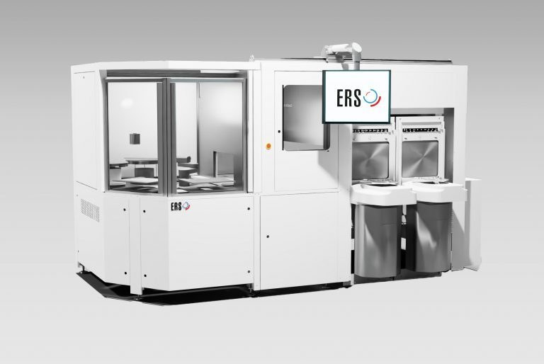
    ERS is giving a first look at the next-generation ADM330
    Bildquelle nicht angegeben
    Semiconductor-packaging

    ERS is giving a first look at the next-generation ADM330

    ERS electronic reveals the details of its third-generation flagship thermal debond machine, ADM330. The machine was introduced to the market in 2007 as
    Veröffentlicht
    08. April 2022
    Lesezeit
    1 Minute
    Rubrik
    Semiconductor-packaging

    ERS is now giving a first look at the next-generation ADM330, which has changed its previously matte metallic appearance to a clean, white surface matching most equipment found in a cleanroom. In addition, the machine is now fully compliant with the GEM300 SEMI standards, thus allowing seamless integration into automated fabs and Industry 4.0 architectures. Warpage adjustment performance has also been improved thanks to a unique thermal chuck design that enables a strong vacuum performance three times better than its predecessor. Lastly, the new ADM330 offers an implemented add-on software feature allowing stand-alone laser marking for improved wafer traceability.

    “We are very excited to reveal the latest upgrade of our flagship machine. With these improvements, we continue to deliver a robust system that meets the ever-changing process requirements of Advanced Packaging,” says Debbie-Claire Sanchez, FO Equipment Business Unit manager at ERS electronic.

    “Fan-out packaging market value is expected to reach more than US$3.4 billion by 2026 at a 14% CAGR 1, mainly driven by 5G, HPC and IoT applications2”, announces Gabriela Pereira, Technology & Market Analyst, Semiconductor, Memory & Computing at Yole Développement (Yole). “In this dynamic context, one of the main technical challenges is the warpage of the reconstituted wafers due to CTE mismatch between the different materials applied. Next-generation of ERS ADM330 debonding equipment announced today by ERS electronic will be a solution to enable warpage adjustment improvement and contribute to reducing yield losses.”


    Mehr aus Semiconductor-packaging

    Weitere aktuelle Artikel aus der Rubrik Semiconductor-packaging.

    Alle Semiconductor-packaging-Artikel
    Nanoscribe Expands Photoresin Portfolio for Micro-Optics Fabrication via Two-Photon PolymerizationFoto: Brecht Corbeel / Unsplash
    Semiconductor-packaging

    Nanoscribe Expands Photoresin Portfolio for Micro-Optics Fabrication via Two-Photon Polymerization

    11. November 2026

    Nanoscribe has detailed its range of photoresins engineered for Two-Photon Polymerization (2PP) and Two-Photon Grayscale Lithography (2GL), targeting high-precision micro-optics manufacturing on silicon, glass, and…

    Canon Launches FPA-6400ES6a KrF Lithography System with 400 Wafers-per-Hour ThroughputFoto: Canon Europe (semicon)
    Semiconductor-packaging

    Canon Launches FPA-6400ES6a KrF Lithography System with 400 Wafers-per-Hour Throughput

    10. November 2026

    Canon has announced the FPA-6400ES6a KrF scanner for semiconductor lithography, combining a throughput of 400 wafers per hour with industry-leading overlay accuracy of 4.0 nm and the ability to handle wafer warpage of…

    Fabmatics absorbs SCI business activities under unified brandFoto: Ludovico Ceroseis / Unsplash
    Semiconductor-packaging

    Fabmatics absorbs SCI business activities under unified brand

    6. November 2026

    Fabmatics has integrated the business activities of SCI under the Fabmatics brand, consolidating the acquired expertise within its semiconductor automation portfolio.

    Entegris and Kioxia Expand Partnership on Materials Innovation for Next-Gen 3D Flash MemoryFoto: Louis Reed / Unsplash
    Semiconductor-packaging

    Entegris and Kioxia Expand Partnership on Materials Innovation for Next-Gen 3D Flash Memory

    6. November 2026

    Entegris and Kioxia are deepening their strategic partnership to co-develop materials and process technologies for future BiCS FLASH 3D NAND architectures, using AI, digital-twin modelling and experimental validation at…

    ← Zurück zu Semiconductor-packagingZur Startseite

