Zum Inhalt springen
EPP Europe
  • News
  • Products
  • Applications
  • Technology
  • Semiconductor
  • Inspection
  • Company News
  • Events
EPP Europe
  • Technology
  • Inspection (AOI/AXI)
  • Semiconductor Packaging
  • Company News
  • Products
  • Trade Shows & Events
    EPP Europe Newsletter
    The most important electronics-manufacturing news delivered to your inbox.

    Info

    • Impressum
    • Datenschutz
    • Barrierefreiheit
    • Datenschutzeinstellungen

    Kontakt zur Redaktion

    EPP EuropeKonradin Mediengruppe
    Ernst-Mey-Str. 8, 70771 Leinfelden-Echterdingen

    E-Mail: redaktion@konradin.de
    Folgen Sie uns
    EPP Europe
    © 2026 EPP Europe
    Startseite/Applications/Artikel
    Copper-Top interconnect technology developed
    Foto: Brecht Corbeel / Unsplash
    Applications

    Copper-Top interconnect technology developed

    IMEC has transferred its Copper-Top (Cu-top) interconnect process technology to National Semiconductor’s production facility in Malacca, Malaysia. The
    Veröffentlicht
    12. April 2007
    Lesezeit
    1 Minute
    Rubrik
    Applications

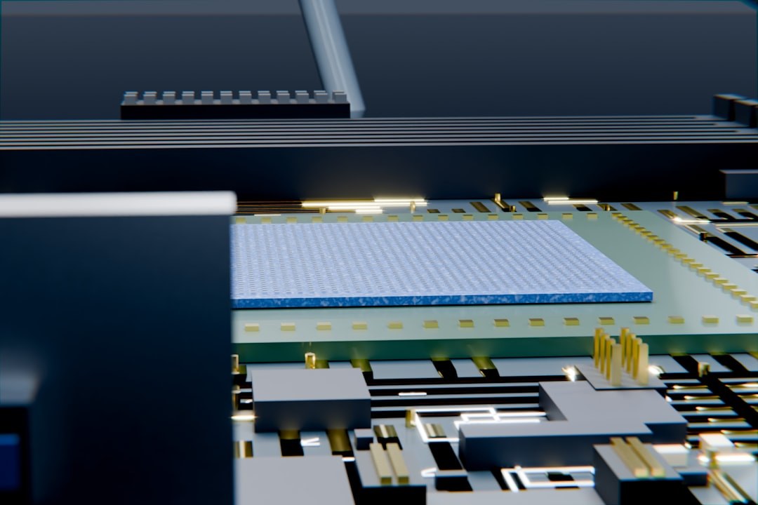
    The Cu-top module can be added to any semiconductor product wafer for current carrying capability. The sheet resistance of the interconnect layer is much lower than today’s standard back-end aluminum (Al) interconnects, therefore, making the technology especially suited for analog and mixed-signal applications where relatively large electrical currents are used. The technology overcomes the resistive voltage drop and power-loss caused by the low conductivity of traditional interconnects resulting in a significant increase of the system efficiency. It prevents the use of wide metal lines and hence reduces chip areas.

    The key feature of this technology is the use of Cu plating in a photoresist pattern, allowing for a small line width to enable a high-density high-current interconnect layer. The contacts through the 2 µm thick IC passivation have a diameter of only 3 µm and have a very good contact resistance between the plated Cu and the underlying Al layer. The Cu layer on the chip is protected by a 10 µm thick polymer dielectric layer. This layer is photo-defined to clear scribe lanes and bonding pads. The Cu bonding pads are covered with an Al metallization to allow for testing and wire-bond packaging.

    The process development and technology transfer results from a three-year close collaboration between IMEC’s thin-film technology group and a team from National Semiconductor Santa Clara, California (USA) and Malacca.

    www.imec.be

    www.national.com

    EPP Europe 468

    Mehr aus Applications

    Weitere aktuelle Artikel aus der Rubrik Applications.

    Alle Applications-Artikel
    Expert to highlight new solder paste in Rosemont
    Applications

    Expert to highlight new solder paste in Rosemont

    25. August 2025

    AIM Solder is participating in the upcoming SMTA International 2025 event, which is taking place from October 19–23 at the Donald E. Stephens Convention

    Selective soldering machine take production to a new level
    Applications

    Selective soldering machine take production to a new level

    27. Mai 2025

    Under the motto “Assembling the Future”, Phonotronica Ltd. has been a pioneer in the development and manufacture of electronic modules since 1990.

    ← Zurück zu ApplicationsZur Startseite