Semiconductors have become an integral part of our networked world. That places great demands on manufacturers as innovation cycles are becoming shorter and shorter while the complexity of integrated circuits is constantly increasing. To remain competitive, there is a particular focus on reducing investment costs and accelerating ramp-up processes to achieve error-free production of new, high-performance components more quickly. The early identification of critical defects considerably accelerates the development and optimization of new production processes and thus the production start-up of new chip generations.
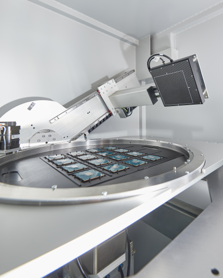
With the CA20 inspection system, Comet Yxlon has taken 3D X-ray technology for the semiconductor Advanced Packaging industry to a whole new level. The complete redesign of the hardware, optimized for semiconductor applications in terms of stability, imaging, precision, and maintenance requirements, combined with high-resolution computed laminography and software packages such as Dose Manager, Batch Manager and ‚Insights‘ for automated evaluations ensure accuracy, reliability, and efficiency for all inspection tasks. All functions are easily and intuitively accessed via the Geminy user interface which has proven itself in the Comet Yxlon FF and UX product ranges, equipped with graphical symbols, wizards, and various presets for every skill level.
„As an accompanying inspection method already in research and development of new microchips and their production processes, the new CA20 will revolutionize the semiconductor industry,“ said Christian Driller, Vice President R&D at Comet Yxlon. „CA20 will ensure that ramp-up processes and time-to- market are dramatically accelerated, the current high scrap rate will get reduced, and yield will thus significantly increase. The system brings the zero-defect goal within reach.“