
Zum Inhalt springen
EPP Europe
  • News
  • Products
  • Applications
  • Technology
  • Semiconductor
  • Inspection
  • Company News
  • Events
EPP Europe
  • Technology
  • Inspection (AOI/AXI)
  • Semiconductor Packaging
  • Company News
  • Products
  • Trade Shows & Events
    EPP Europe Newsletter
    The most important electronics-manufacturing news delivered to your inbox.

    Info

    • Impressum
    • Datenschutz
    • Barrierefreiheit
    • Datenschutzeinstellungen

    Kontakt zur Redaktion

    EPP EuropeKonradin Mediengruppe
    Ernst-Mey-Str. 8, 70771 Leinfelden-Echterdingen

    E-Mail: redaktion@konradin.de
    Folgen Sie uns
    EPP Europe
    © 2026 EPP Europe
    Startseite/Semiconductor-packaging/Artikel
    CITC and Henkel forge partnership to accelerate high-thermal die attach solutions
    Bildquelle nicht angegeben
    Semiconductor-packaging

    CITC and Henkel forge partnership to accelerate high-thermal die attach solutions

    Chip Integration Technology Center (CITC) and Henkel announced today that the organizations have formalized an agreement to collaborate on the development
    Veröffentlicht
    22. Juli 2022
    Lesezeit
    2 Minuten
    Rubrik
    Semiconductor-packaging

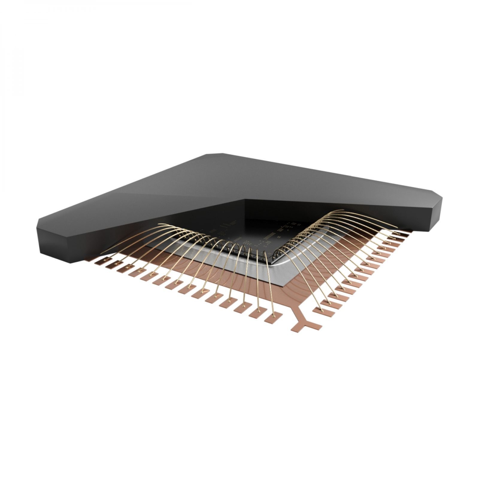
    CITC’s Thermal High-Performance Packaging program focuses on thermo-mechanical design strategies and device packaging platforms that integrate low-stress, high-reliability rugged interconnect solutions. As die attach and molding materials are often limiting factors for the optimal operation of RF and power packages, Henkel is the ideal partner or innovation in this application area.

    In addition to ongoing work in its state-of-the-art R&D centers, Henkel wants to accelerate time-to-market for its semiconductor packaging materials through strategic relationships across industry, government, and academia. CITC, which collaborates with leading power and RF device packaging companies, provides a unique opportunity to characterize and analyze Henkel’s high-thermal die attach formulations as an enabler for leading-edge device designs.

    “Henkel’s pressureless sintering die attach materials are already proven in certain mobile applications,” explained Ramachandran “Ram” Trichur, the company’s Global Market Segment Head, Semiconductor Packaging Materials. “We want to extend that success to other sectors such as automotive, where large, high-power chips are the norm. Our pressureless sintering solutions are unique because they deliver the simple, low-stress processability of conventional die attach adhesives and very high thermal conductivity capabilities. The work at CITC will augment our in-house projects, allowing additional performance and reliability validation.”

    The new die attach technology has the potential to enable the replacement of lead (Pb) within RF and power semiconductor devices that incorporate larger die on copper leadframes, allowing the introduction of high operating temperature gallium nitride (GaN) and silicon carbide (SiC) power die technologies. Many of CITC’s partners are actively integrating these new chip structures, making the cooperative project an excellent proving ground for Henkel’s pressureless sintering platform.

    “In Henkel, we have found a material innovator that will enable the development of power and RF devices with a holistic approach that leverages the latest in die attach technology,” concluded CITC General Manager, Jeroen van den Brand. “With many major power device manufacturers based in Europe, and in Nijmegen in particular, we view this partnership as vital to satisfying the current and future demands within these important market sectors.”


    Mehr aus Semiconductor-packaging

    Weitere aktuelle Artikel aus der Rubrik Semiconductor-packaging.

    Alle Semiconductor-packaging-Artikel
    Nanoscribe Expands Photoresin Portfolio for Micro-Optics Fabrication via Two-Photon PolymerizationFoto: Brecht Corbeel / Unsplash
    Semiconductor-packaging

    Nanoscribe Expands Photoresin Portfolio for Micro-Optics Fabrication via Two-Photon Polymerization

    11. November 2026

    Nanoscribe has detailed its range of photoresins engineered for Two-Photon Polymerization (2PP) and Two-Photon Grayscale Lithography (2GL), targeting high-precision micro-optics manufacturing on silicon, glass, and…

    Canon Launches FPA-6400ES6a KrF Lithography System with 400 Wafers-per-Hour ThroughputFoto: Canon Europe (semicon)
    Semiconductor-packaging

    Canon Launches FPA-6400ES6a KrF Lithography System with 400 Wafers-per-Hour Throughput

    10. November 2026

    Canon has announced the FPA-6400ES6a KrF scanner for semiconductor lithography, combining a throughput of 400 wafers per hour with industry-leading overlay accuracy of 4.0 nm and the ability to handle wafer warpage of…

    Fabmatics absorbs SCI business activities under unified brandFoto: Ludovico Ceroseis / Unsplash
    Semiconductor-packaging

    Fabmatics absorbs SCI business activities under unified brand

    6. November 2026

    Fabmatics has integrated the business activities of SCI under the Fabmatics brand, consolidating the acquired expertise within its semiconductor automation portfolio.

    Entegris and Kioxia Expand Partnership on Materials Innovation for Next-Gen 3D Flash MemoryFoto: Louis Reed / Unsplash
    Semiconductor-packaging

    Entegris and Kioxia Expand Partnership on Materials Innovation for Next-Gen 3D Flash Memory

    6. November 2026

    Entegris and Kioxia are deepening their strategic partnership to co-develop materials and process technologies for future BiCS FLASH 3D NAND architectures, using AI, digital-twin modelling and experimental validation at…

    ← Zurück zu Semiconductor-packagingZur Startseite

