Microelectronics is the main drive behind the technological progress of the last decades. With each level of miniaturisation electronic devices not only become smaller, but also more powerful, new applications and opportunities arise. At the beginning of this process in the mid-1960s, electronics pioneer Gordon Moore stated his famous law according to which the number of components in a computer chip doubles every one and a half years. This statement has been valid ever since then and experts judge that it is going to be so for at least ten or fifteen years. Meanwhile, miniaturisation has reached the nanometre level demanding high-precision equipment for the production of microchips. One key step in the production chain is lithography.
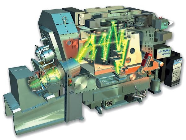
The joint technological achievements of both companies grant their leadership in this very specialised market, where success depends on the amount of miniaturisation the optical equipment can achieve. At the moment, ASML’s immersion technology reaches the highest resolution. The newly developed EUV technology, using extreme ultra violet light, is currently tested in two prototype machines in Belgium and the US (figure 1).
The core element of each lithography platform is its optical column, which consists of an excimer laser light source, followed by an illuminator to shape the beam. Different beam shapes like quadrupoles, ring or circular, are used to optimally illuminate different kinds of chip structures. The pattern mask or reticle that is to be printed on the silicon is inserted between the illuminator and the object lens that is used to scale down the patterns to one quarter of the size on the mask.
Resolution of lithographic stepper scanners follows the formula dmin = k1 · l/NA with dmin signifying the minimum feature size that can be achieved. The main factors that can be influenced by the optical technology are l, the wavelength of the light, and the numerical aperture NA. The second value defines the range of angles over which the system is able to accept or emit light. Consequently low wavelength light and a high aperture are required to reach the smallest possible detail size. The so-called process factor k1 is depending on the detailed processes set up by the chip manufacturer. This factor cannot reach levels below 0.25. However – the lower k1, the more susceptible the whole production process becomes for even least variations of for example laser power, optical aberrations, temperature etc. Standard machines use process factors between 0.3 and 0.5.
The main factor to define NA is the half angle of the light cone between the lens and the focus point on the wafer for air as optical medium between the last lens element and the wafer. Therefore mathematically, NA increases in correlation with the lens radius. In practise, larger lenses accept more light. In order to assure a low level of aberrations (below 1 nm rms) more lenses are applied as well as lenses with aspherical surfaces. Meanwhile, optical lenses of standard lithography scanners consist of an assembly of up to 20 lens elements, the largest of which are over 30 cm in diameter. As a consequence these projection lenses are 1.3 meters high and weigh more than a metrical ton. Carl Zeiss SMT has to coat the various lenses with special antireflective materials. Else there would be so many reflections that hardly any light is left to reach the wafer. These lenses deliver apertures of 0.93, which is very close to the theoretical maximum of 1 for air as a surrounding medium. They reach a resolution of less than 65 nanometres.