Zum Inhalt springen
EPP Europe
  • News
  • Products
  • Applications
  • Technology
  • Semiconductor
  • Inspection
  • Company News
  • Events
EPP Europe
  • Technology
  • Inspection (AOI/AXI)
  • Semiconductor Packaging
  • Company News
  • Products
  • Trade Shows & Events
    EPP Europe Newsletter
    The most important electronics-manufacturing news delivered to your inbox.

    Info

    • Impressum
    • Datenschutz
    • Barrierefreiheit
    • Datenschutzeinstellungen

    Kontakt zur Redaktion

    EPP EuropeKonradin Mediengruppe
    Ernst-Mey-Str. 8, 70771 Leinfelden-Echterdingen

    E-Mail: redaktion@konradin.de
    Folgen Sie uns
    EPP Europe
    © 2026 EPP Europe
    Startseite/Products/Artikel
    Blind, buried vias, stacked microvias with laser drilling
    Bildquelle nicht angegeben
    Products

    Blind, buried vias, stacked microvias with laser drilling

    Rush PCB Inc. announces quick-turn PCB fabrication for production and prototypes, with particular demonstrated expertise in challenging multilayer board
    Veröffentlicht
    27. April 2015
    Lesezeit
    1 Minute
    Rubrik
    Products

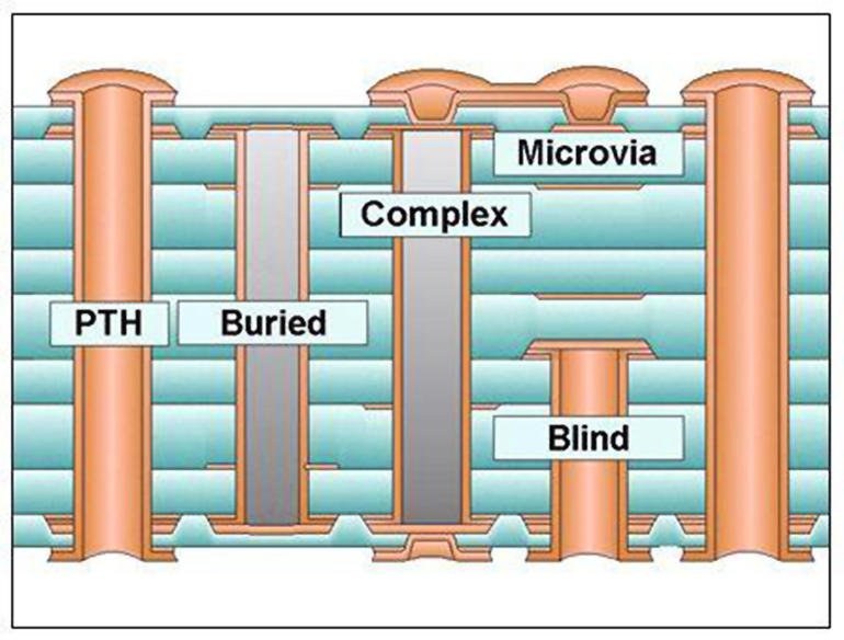
    Blind vias are originate on an outer layer but terminate at an inner layer; buried vias exist only between inner layers and do not begin or terminate on an outer layer, so they must be drilled while layers are being added to the PCB rather than when it is finished.

    Stacked microvias, compound structures, are stacked one on top of another as to achieve the highest possible routing density. Laser-drilled micro-vias reduce the space consumed by through-the-board vias. Micro-vias, having been drilled by laser, are smaller in diameter than through-vias, and because they’re smaller, more space can be devoted to circuit traces. A micro-via links only one layer of foil to the next; layers above and below these are available for foil lines, further increasing overall circuit density.

    The company can fabricate stacked micro vias (HDI), boards up to 48 layers, and oversized Boards. 4 mil laser drill capability allows for ultra-fine features to be produced, Roy Akber, CEO says. “But we emphasize that we can help customers with these types of space-saving features if they come to us at the beginning of the design stage for their product,” he says. “We provide a full spectrum of engineering and design support, and can help customers find more economical ways to do certain things, such as impedance control. We have ready-to-go proven designs in house that can be immediately applied to a customer’s needs. Our goal is ultimate reliability for the customer’s products.”

    www.rushpcb.com

    Mehr aus Products

    Weitere aktuelle Artikel aus der Rubrik Products.

    Alle Products-Artikel
    Heavy board options added to reflow soldering system
    Products

    Heavy board options added to reflow soldering system

    27. Mai 2025

    Provider of reflow soldering technology, Vitronics Soltec has launched new Heavy Board options for its Centurion 1240 reflow soldering system. This

    New 3D AXI platform provides clearer imaging
    Products

    New 3D AXI platform provides clearer imaging

    22. Januar 2025

    Test Research, Inc. (TRI) has announced the launch of its new 3D AXI TR7600FB SII system and emphasized that it has been designed to deliver clearer

    No-clean formula maximize the solderability
    Products

    No-clean formula maximize the solderability

    10. Januar 2025

    Indium Corporation announced the global availability of CW-807RS, a new high-reliability, halide- and halogen-free flux-cored wire that improves wetting

    Extensive program of testing options
    Products

    Extensive program of testing options

    10. Januar 2025

    Test Research, Inc. (TRI) will join the IPC APEX EXPO 2025 held at Anaheim Convention Center on March 18 – 20, 2025 at booth #2905 to show latest test and

    ← Zurück zu ProductsZur Startseite