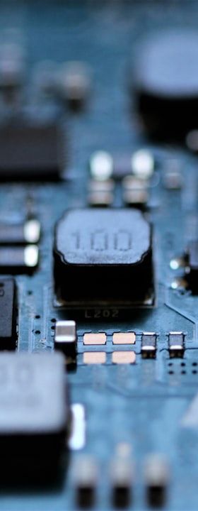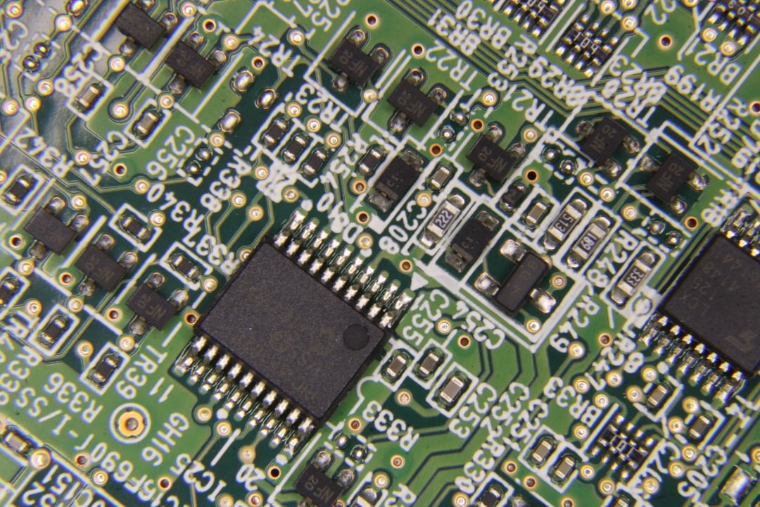
As PCB assemblies grow denser and component geometries shrink toward 01005 and µBGA dimensions, manual visual inspection has long ceased to be a viable quality gate. Automated Optical Inspection — universally abbreviated as AOI — fills this role by combining structured illumination, high-resolution imaging and image-processing algorithms to evaluate populated boards at production speed. The technology is deployed at multiple points in the SMT process: after solder paste printing (though that function is more specifically addressed by dedicated SPI systems), after component placement and, most critically, after reflow soldering. Each inspection point targets a distinct defect spectrum and requires correspondingly adapted optical and algorithmic configurations.
The global adoption of AOI is driven not merely by the limitations of human vision but by the statistical demands of modern production. A single automotive control unit may carry several thousand solder joints; even a defect rate of 50 ppm translates into measurable field failures at volume scale. AOI provides the combination of speed, repeatability and objective documentation that manual inspection fundamentally cannot offer.
Optical Architecture: Illumination, Optics and Sensors
The performance of an AOI system is determined in large part by its illumination strategy. Most contemporary systems employ multi-angle LED ring illuminators arranged in concentric zones, each zone radiating light at a defined elevation angle. By capturing images under different illumination conditions — high-angle for specular surfaces such as solder fillets, low-angle for detecting coplanarity deviations — the system extracts complementary information that a single illumination direction would conceal. Coloured LED segments (typically red, green and blue at different angles) enable pseudo-3D reconstruction of surface topography through the photometric stereo principle, even in systems that are primarily classified as 2D.
True 3D AOI systems, which have become the production standard for high-complexity assemblies, supplement or replace photometric stereo with structured light projection. A fringe pattern — usually a sinusoidal intensity grating — is projected onto the board surface and the phase shift of the distorted pattern is evaluated by triangulation. This yields a dense point cloud from which component height, coplanarity and solder volume can be quantified, not merely inferred from grey-value contrast. Sensor resolution in current systems ranges from below 10 µm per pixel for fine-pitch applications down to 5 µm and below for advanced packaging inspection, necessitating either large-format CMOS sensors or multi-camera tile-scanning approaches.
Defect Detection: Algorithm Classes and Their Trade-offs
Early AOI systems relied primarily on template matching: a stored reference image of a known-good assembly was compared pixel-by-pixel to the acquired image, with deviations beyond a threshold flagged as suspect. While computationally straightforward, pure template matching is highly sensitive to board-to-board colour variation, surface oxidation and component lot changes — all of which generate pseudo-defects. The industry response was the development of rule-based inspection, where each component type is evaluated against parametric rules: fillet height within defined bounds, component body within placement tolerance, polarity marker aligned to the design database.
Contemporary systems increasingly incorporate machine-learning classifiers, typically convolutional neural networks trained on large labelled defect libraries. These classifiers operate downstream of the geometric measurement stage to reduce false calls: a solder joint that fails a dimensional threshold is re-evaluated by the classifier before being escalated to an operator. The practical effect is a significant reduction in false-call rate — a chronic problem in AOI that directly determines operator workload and the credibility of the inspection gate. The training datasets must, however, represent the actual defect morphology of the target process; a model trained on tin-lead solder images will generalise poorly to SAC305 fillets with their characteristically different grain structure and surface texture.
Inline Integration: Placement within the SMT Process Flow
Post-reflow AOI is the most widely implemented inspection point and addresses the broadest defect spectrum: open circuits, bridging, insufficient or excessive solder, tombstoning, component shift, missing or wrong components and polarity reversal. The system is positioned immediately downstream of the reflow oven and upstream of any depanelling or manual touchup station, ensuring that defective boards are identified before further value is added.
Post-placement AOI — sometimes called pre-reflow or mid-line AOI — targets placement defects before they are committed through soldering. Detecting a missing component or a shifted µBGA at this stage is considerably cheaper than discovering it after reflow, where rework is both time-consuming and thermally stressful to the assembly. The trade-off is that inspecting an unsoldered board requires the system to assess component presence and orientation without the reference of the solder fillet, relying instead on body and pad geometry. Throughput must also be matched to the placement machines feeding the line, which in high-volume environments can exceed several thousand components per hour.
Closed-loop feedback integration is an increasingly important capability. When the AOI system detects a systematic offset — for example, a consistent placement shift on a specific nozzle or feeder position — it can communicate corrective data upstream to the placement machine or SPI system via a standardised interface, enabling process correction before the deviation exceeds the reject threshold. IPC-CFX (Connected Factory Exchange) and SMEMA electrical interfaces are the primary integration frameworks in current use.
Programming, False-Call Management and Ongoing Optimisation
AOI programming — defining the inspection rules, regions of interest and acceptance thresholds for each component — remains one of the most labour-intensive aspects of system deployment. Offline programming tools that import CAD and BOM data automatically generate a first-pass inspection programme, but threshold optimisation invariably requires iterative refinement against real production data. The goal is to achieve a receiver operating characteristic that minimises both escape rate (defects passing the inspection gate) and false-call rate simultaneously; these objectives are in tension, and the optimal operating point depends on the downstream consequences of each error type.
Statistical process control integration provides the long-term mechanism for threshold management. By tracking measurement distributions over time, engineers can detect process drift — gradual changes in solder volume, placement accuracy or component geometry — before the process crosses reject boundaries. This transforms AOI from a binary pass/fail gate into a continuous process monitoring tool, consistent with the data-driven quality philosophy of IPC-A-610 and related standards.
Limits of AOI and Complementary Inspection Technologies
AOI is inherently a line-of-sight technology. Solder joints hidden beneath components — BGA, LGA, QFN and flip-chip packages — are not accessible to optical methods regardless of illumination sophistication. For these package types, Automated X-ray Inspection (AXI) is the appropriate technology, using X-ray attenuation contrast to image subsurface solder joints. In practice, most high-complexity lines deploy both AOI and AXI as complementary layers, with AOI handling the majority of inspectable joints at line speed and AXI addressing area-array packages either inline or in a sampling regime.
Similarly, AOI verifies geometric and visual attributes but provides no information about electrical functionality. Electrical test methods — In-Circuit Test and flying-probe — remain necessary where functional verification is required. The trend in advanced manufacturing is toward integrated traceability architectures in which AOI, AXI, SPI, ICT and functional test data are aggregated per board serial number, enabling failure mode correlation and root-cause analysis across the full process chain. This systemic view, rather than the standalone capability of any individual inspection technology, defines the direction of quality engineering in electronics manufacturing.