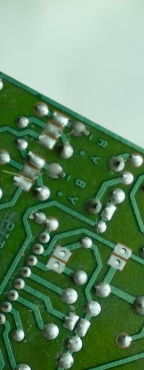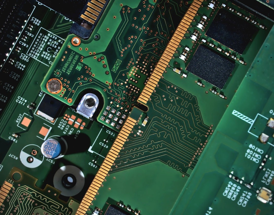
As component densities increase and solder joint geometries shrink, manual visual inspection has long ceased to be a viable quality assurance strategy in high-volume SMT manufacturing. Automated Optical Inspection — universally abbreviated as AOI — fills this role by capturing and analysing images of populated circuit boards at line speed, flagging deviations from a defined reference state. What began as a relatively simple 2D image-comparison tool has evolved into a multi-camera, multi-angle, sometimes three-dimensional measurement system deeply embedded in the manufacturing execution workflow. For process engineers and quality managers alike, a clear understanding of how AOI systems work, what they can and cannot detect, and where they belong in the assembly sequence is prerequisite knowledge for building a robust, zero-defect production strategy.
AOI is not a single technology but rather a family of optical measurement approaches that share a common architecture: structured illumination, one or more image sensors, and a software engine that compares captured data against a stored reference or a rule-based defect library. The specific implementation — camera count, lighting geometry, image resolution, inspection algorithm — determines the system's capability profile and its suitability for a given assembly type.
Optical Architecture: 2D, 2.5D and 3D Systems
Classic 2D AOI systems use a single top-down camera combined with coaxial or ring-shaped illumination. The captured greyscale or colour image is compared pixel-by-pixel or region-by-region against a golden-board reference or a CAD-derived template. While computationally straightforward and fast, pure 2D inspection is inherently limited: it cannot measure component height, solder joint volume or coplanarity deviations. It detects presence, absence, polarity and gross positional errors reliably, but struggles with lifted leads or insufficient solder that does not manifest as a visible surface anomaly.
2.5D systems supplement the top-down camera with angled side cameras — typically four cameras arranged at 45-degree angles around the optical axis, sometimes supplemented by additional oblique views. This multi-angle architecture makes solder fillet geometry visible and allows height estimation through shadow analysis or photometric stereo methods. Many mid-range production AOI systems currently on the market fall into this category.
True 3D AOI systems use structured-light projection — most commonly laser triangulation or fringe projection (phase-shift moiré) — to generate a full three-dimensional height map of the board surface. This enables absolute measurement of component height, coplanarity, solder paste volume on already-placed components, and subtle lifted-lead conditions. The trade-off is cycle time: acquiring and processing a dense point cloud is computationally more demanding than processing a 2D image, though modern systems have largely closed this gap through parallel processing architectures and dedicated FPGAs.
Illumination Design and Its Influence on Defect Visibility
Illumination is often the decisive factor in whether a specific defect class is detectable. Coaxial illumination — where light travels along the same axis as the camera — produces strong specular reflections from flat metallic surfaces and is useful for detecting solder bridging and missing components. Dome illumination distributes light from all angles simultaneously, minimising shadows and specular artefacts, making it well suited for inspecting highly reflective BGA pads and fine-pitch QFP leads.
Structured colour illumination — using LED rings with segments emitting red, green and blue light at different elevation angles — encodes height information as colour gradients in the captured image. A solder fillet that rises steeply toward a component lead will appear as a transition from blue (low angle, base of fillet) to red (high angle, near lead) in the composite image. This technique, sometimes called multicolour illumination or colour highlight inspection, provides pseudo-3D information at 2D acquisition speeds and is widely deployed in inline post-reflow AOI.
Programme Creation, False-Call Rate and Pseudo-Error Management
The practical value of an AOI system is determined not only by its optics but also by the quality of its inspection programme and the discipline of its programme maintenance. Inspection programmes define, for each component on the board, the measurement windows, reference values, tolerances and defect classification rules. Programme creation can be CAD-driven — importing centroid files, BOM data and Gerber layers — or taught from a physical golden board. Modern systems offer automated programme generation (APG) pipelines that reduce initial setup time substantially.
False calls — instances where the AOI system flags a correctly assembled board as defective — are the most operationally disruptive quality metric in AOI operation. A high false-call rate burdens repair stations with unnecessary rework, reduces throughput and, critically, erodes operator trust in the system, leading to systematic override behaviour that defeats the purpose of inspection. Managing false calls requires iterative tolerance tuning, component library maintenance, and a structured feedback loop from the repair station back to the AOI programme. Industry practice distinguishes between the false-call rate (incorrectly rejected good boards) and the escape rate (accepted boards with actual defects); both must be tracked.
Statistical process control integration — where AOI measurement data feeds directly into SPC charts monitoring positional drift, solder volume trends or component placement offset — transforms the AOI from a pass/fail gate into a process monitoring tool. Detecting a gradual offset trend in QFP placement before it crosses the defect threshold allows corrective action without generating rejects.
Placement in the Assembly Line: Pre-Reflow vs. Post-Reflow AOI
AOI can be deployed at multiple points in the SMT assembly sequence, each with a different inspection focus. Post-paste-print AOI — technically overlapping with Solder Paste Inspection (SPI) when combined with 3D measurement — verifies paste deposit geometry before component placement. Pre-reflow AOI, positioned after the pick-and-place machine and before the reflow oven, inspects component placement accuracy, polarity and presence. Defects caught at this stage can be corrected before soldering, dramatically reducing rework cost.
Post-reflow AOI is the most common deployment point and inspects the final soldered assembly. It is the primary quality gate before board-level test and, in many lines, before conformal coating or box build. Some advanced lines deploy AOI after wave or selective soldering as well, particularly for mixed-technology assemblies where through-hole solder joints require optical verification.
Integration with MES, Traceability and Closed-Loop Feedback
Modern AOI systems communicate bidirectionally with the manufacturing execution system via standardised interfaces — IPC-CFX (Connected Factory Exchange) and SMEMA are the most prevalent in SMT environments. Each inspected board is linked to its serial number or DMC (Data Matrix Code), and the inspection result, including the list of flagged components with coordinates and defect classification, is written to the MES database. This creates a per-unit quality record that supports full product traceability, a requirement in automotive (IATF 16949), medical (ISO 13485) and aerospace (AS9100) manufacturing.
Closed-loop feedback takes integration a step further: aggregated AOI data is analysed to identify systematic placement errors attributable to specific nozzles or feeders in the pick-and-place machine, and correction offsets are automatically transmitted back to the placer. Similarly, persistent solder-bridge patterns at a specific pad geometry can trigger an automated stencil inspection or squeegee pressure review. This feedback architecture is the operational backbone of what the industry broadly refers to as smart factory or Industry 4.0 assembly — replacing reactive quality control with predictive, data-driven process management.
Practical Considerations and Technology Selection
Selecting an AOI system requires matching the system's optical resolution, field of view, throughput and programme flexibility to the specific assembly mix. A contract manufacturer running high-mix, low-volume production demands rapid programme changeover and robust CAD import; a high-volume automotive supplier prioritises throughput and SPC integration. Component miniaturisation — with 01005 passives and 0.3 mm-pitch BGAs now commonplace — demands camera resolutions of 10 µm per pixel or better in the region of interest, achievable either through high-resolution fixed cameras or through resolution-on-demand zoom optics.
As assemblies incorporate more complex packages — embedded components, system-in-package modules, double-sided boards with high component shadows — the limits of optical inspection become apparent and AOI is increasingly complemented by Automated X-ray Inspection (AXI) for hidden joint verification. Understanding the respective detection envelopes of both technologies, and designing an inspection strategy that deploys each where it offers the highest return, remains one of the core competencies of modern SMT quality engineering.