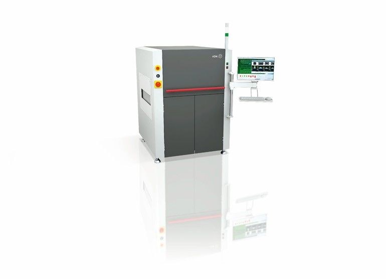
“With the new ASM ProcessLens, ASM combines the need for maximum precision from the semiconductor field with the speed requirements in SMT production,” said Jérôme Rousval, ASM Solutions Marketing Manager and specialist for SPI systems. “Users no longer need to accept a compromise with this system, which allows them to produce with more flexibility, efficiency and productivity than ever before. And when they use the option to expand it to the world’s first self-learning ASM Process Engine system, they have reached a fundamental milestone on the road to the Integrated Smart Factory.”
“With the new ASM ProcessLens, speed and precision are no longer mutually exclusive but combined in a single machine,” the company added. “To inspect a standard board with an area of approx. 69,000 square millimeter and more than 6,020 pads, the totally new SPI system from ASM takes only 3.0 seconds in high-speed mode or 3.7 seconds in high-resolution mode with resolutions of 20 and 10 microns, respectively.”
“Covering 50 by 50 millimeters (2,500 sq.mm), the scanning area of the 26-megapixel camera is 277 percent larger than the previous version’s with 4 megapixels and 30 by 30 millimeters. The number of micro-mirrors on the DLP (Digital Light Projector) chip that generates the moiré patterns was increased from 8 million to 20 million for a much higher resolution by cutting each mirror’s size roughly in half. Each mirror is electronically controllable so that the stripe patterns can be projected completely vibration-free without any movement of the light source.”
The DLP chip is controlled by a completely new generation of algorithms that generate the moiré patterns much more quickly and precisely. The time required to change the mirrors’ positions to generate the stripes is 16 microseconds. In addition, test programs can now be exchanged between machines and platforms. The same applies to important machine characteristics such as camera rotation. When these properties are transferred to another machine, the software adjusts them automatically in order to ensure the same quality of measurement results.
Focus on accuracy
“Another focus area was the development and refinement of the control mechanisms for accurate operation in the microsecond range,” the company added. “Vibrations from other areas of the inspection system are balanced out, and light control is optimized by compensating for delays until full luminance has been achieved. ASM has also made improvements to the system’s thermal stability because only if all optical elements of the ASM ProcessLens are immune to thermal factors can even the smallest distortions in the recorded images be excluded. All elements are manufactured with a 3D printing process, and no part gets accepted if it has a less than 99-percent reliability rating. And to optimize the heat management in the machine, the heat dissipation system was redesigned from the ground up.”