Today, productivity is particularly important for every company to be responsive and produce quickly, in order to be able to deliver to customers as quickly as possible. Manufacturers are interested in all possible methods of accelerating production. In the 1980s, UV curing process started to be used through a chemical formulation (including photo initiators), a polymerization reaction (curing) is carried out via the UV light received by the substance (liquid). The main advantage of this technology is the speed of polymerization, a few seconds are sufficient!
The advantage can be substantial, especially in terms of storage, because at the end of the production line, products can be handled so they can be packaged and sent directly to the customer. The size of industrial lines can be reduced by replacing IR ovens (3 to 6 meters long used for solvent based materials) with significantly shorter UV ovens (0.8 to 2 meters) that will consume less energy. UV curing technology is booming in the electronics market, but it is still in its infancy.
Several hurdles have slowed its development.
First, it was related to the shadow areas on some PCBs where the coating can penetrate but not receive any UV light, limiting its polymerization.
The purchase of a new oven with new technology can also be a hurdle, as the electronics industry often favours proven technologies that have decades of testing and feedback. Nevertheless, different players (chemical and equipment manufacturers) are pushing UV technology, to draw studies and feedback from experiments, because the market and industry are moving in the direction of this technology for the different curing processes in electronics.
The ABchimie laboratory has been able to develop UV dual cure conformal coating materials that meet the constraints and standards of the electronics market to protect PCBs using a faster process and with a lower environmental impact.
As a reminder, UV curable conformal coating material does not contain solvents, so there is no VOC (Volatile Organic Compound). Nowadays, there are two technologies for the UV curing processes: mercury lamps or UV LED lamps. So how to choose?
Mercury lamps are the most proven systems, cheaper (lamps alone) and still represent 80 % of the UV curing market (any industry). In the long term, as environmental standards evolve (REACH for example), they will surely disappear (by 2030/2040). UV LED lamps first appeared in the early 2000s and began to have sufficient UV power (for industrial UV curing applications) in the early 2010s.
What is a Mercury lamp?
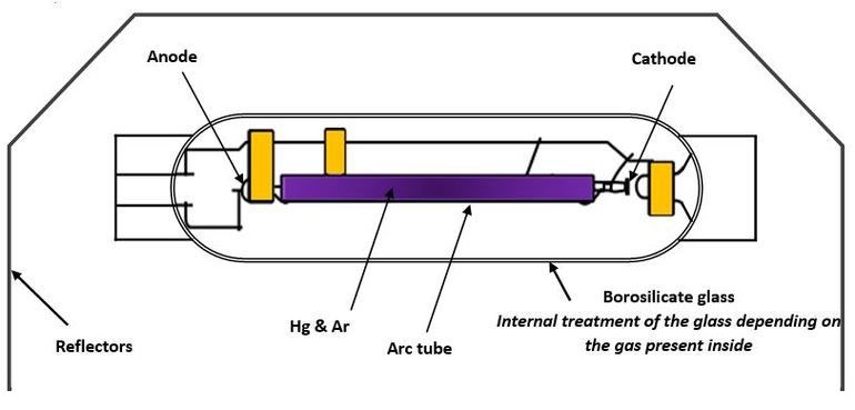
The operating principle is the following: a current passes through the gases in the arc tube, and light will be emitted by ionizing the photons. The wavelength will depend on the gases present in the lamp. Mercury is often present in the form of „small beads“ and when heated will end up in the gas state to mix with the other inert gas present in the tube. There are also lamps doped with iron or gallium. This will depend on the wavelengths and the spectrum of light that is needed. For example, the spectrum of a gallium doped lamp is close to the spectrum of a UV LED lamp (around 400 nm).
Around the lamp, optical reflectors focus the rays at a certain working distance to optimize optical power. This distance must be known to optimize a UV curing process. Cleaning the reflectors should be done frequently, to not lose too much optical power due to the dirt that could be found on the reflectors. They are also tasked with recovering the rays emitted in the wrong directions, because the emission is 360 degrees to recover the maximum of the optical flow.
The lifespan of a mercury lamp varies from 600 to 2000 hours. Knowing that a mercury lamp needs a heating time that can vary from a few minutes to more than 10 minutes, this generates periods when the mercury lamp is on but is not used. It should be kept in mind that they are not made to be turned on and off frequently, as it will shorten their lifespan.
The light spectrum of a mercury lamp is often wide, meaning that several wavelengths are emitted, UVA, UVB and UVC. UVC is a powerful (and dangerous) UV ray that facilitates UV curing of chemical formulations. They will particularly help with the surface cure of the conformal coating. But these rays will split the oxygen molecules present in the air (O) to create ozone (O2, harmful and dangerous gas), so an ozone extraction system is necessary in the curing equipment.
The efficiency of a mercury lamp is in the order of 5 %, which means that, for 100W consumed, only 5W are converted into optical power. In addition, since it has a wide spectrum, only a portion of the wavelengths emitted are useful for the UV curing reaction. The visible wavelengths emitted are not used for polymerization. Also 70 % of the power emitted is infra-red, it is „direct heat emission“, which can weaken certain electronic components or sensitive plastic parts.
The power of a mercury lamp decreases over time depending on its use, which means that it must regularly control its power to be sure that the dose in millijoules is sufficient to ensure correct and sufficient curing. This is a constraint to be considered in the choice of a technology.
The price of a mercury lamp is rather attractive (a few hundred euros), but this system requires a lot of maintenance and users must have in mind that it is necessary to replace the lamps quite frequently. REACH and other environmental standards that do not promote the sustainability of this technology must also be considered. In addition, the integration of a mercury lamp into an equipment requires an extraction system and temperature management that can be quickly binding.
What is a UV LED lamp?
The operating principle is the following: a current passes through the semiconductor materials. The electrons passing from one junction (N and P) to another will lose energy which will create a photon (active zone) and thus emit light. For this technology, it is the choice of semiconductor materials that will determine the wavelength emitted by the LED. A UV LED lamp, therefore, is an electronic system that includes several LEDs (sometimes thousands) depending on the size of the emission window and the optical power to be obtained. For example, a 395 nm UV LED lamp means that all UV LEDs used are the same and that their main property is to have their emission peak at 395 nm.
For a UV LED curing reaction, the chemistry must be properly dedicated to the wavelength emitted by the system, because if all the optical power sent does not correspond to the wavelength of the photo initiators, the polymerization reaction will not start.
For a UV LED system, working distance can sometimes be problematic. Indeed, an optical system is not always available to reduce optical power losses for long working distances. If the UV power is too low, the chemical reaction may also not be fully completed. ABchimie and its partners have worked hard to offer more efficient chemical solutions and UV LED lamps to keep great flexibility on UV LED curing processes.
The lifespan is around 20,000 hours, which means , it can be used 24/7 through out a 2 year period. Knowing that LED technology has on/off flexibility, this allows for it to be used only when needed. There is no heating time (a few hundred microseconds), so an UV LED lamp can used when material needs to be cured. In relation to a production, these „2 years“ can easily be transformed to 5 years or more, without maintenance or replacement of the UV LED lamp.
The spectrum of a UV LED system is often very narrow (for example, a main peak at 395 nm plus or minus 10 nm), often in UVA. These are the least dangerous UV, but because of their power, they do remain dangerous. There is no creation of ozone because there is no presence of UVC. The heat stress emitted is also less important because there is no IR emitted by this type of UV LED system.
The efficiency of this type of system is around 30 %, which means that for every 100W consumed, 30W are optical power. Meaning, this is normally used directly for UV curing, since the chemistry is adapted to the wavelength emitted by the LED lamp.
To measure an UV LED system, all that is needed is a radiometer calibrated in the wavelength emitted by the UV LED system. The irradiance and energy directly used for the curing process is measured, which is repeatable and stable. The UV LED system loses little or no irradiance over time. It is a guarantee of safety.
The price of a UV LED lamp is often higher than a mercury lamp system: the order of magnitude is several thousands of euros. This price is to be linked to its lifespan, its energy gains, its flexible on/off function, its low maintenance and its low environmental impact. The integration of this type of lamp does not pose any problems and allows users to dispose of ovens at competitive prices.
Rethinking production lines
UV curing applications in electronics do not stop at conformal coating materials. There are also UV resins or UV gels available to form barriers before the coating is applied, thus preventing the coating from migrating under components or on areas of the PCBA which should not be coated. For the curing of resin cord or gel, UV LED technology has several advantages. Indeed, a UV LED spot can be mounted allowing an almost immediate curing of the material after application. It is simple and effective.
However, it is necessary to keep in mind the hazards related to these UV rays to offer well-secure and ergonomic machine/material couples for general users and electronics manufacturers. The evolution of chemistry and technologies will move towards greener technologies with low-temperature UV LED curing processes, without VOCs.
For this purpose, the company PPE (Product Process Expertise) has developed a lamp that the company MStech, via SMT Worldwide, already offers equipment, meeting these strict requirements and allowing, through a differentiated process, to cure materials even at distances up to 20 cm high. This gives a stable process with a well thought out equipment with options that allow the traceability of each PCB.
ABchimie
1230, route de la porte
ZA La Rivoire
38630 Corbelin France
Tel.: +33 474 83 12 19
E-Mail: info@abchimie.com
Website: www.abchimie.com
Alexandre Veilly, Sales Manager France – ABchimie