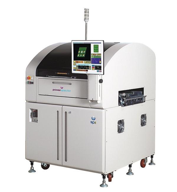
The S1 mkII is capable of defect detection beyond anything previously possible, because it incorporates patented sensor technology that can simultaneously combine 2D and 3D image processing. The new technology allows a vast reduction of wide inspection tolerances, typical of most SPI systems. True area, shape, volume, offset and height measurements are provided in combination, providing genuine yield enhancing process control and a perfect tool to tune and monitor printer settings before a problem spreads throughout an entire production run.
Jeremy Saise, Mek Technical Director further explained, “This is a revolutionary, process control tool that enables users to quickly and easily tune and adjust their print process. We have introduced Production Control Mode. You see, most SPI are utilized only to improve process control, and are left with wide tolerances to accommodate varied paste releases. The Mek S1 can automatically understand these varied releases and bring the real world of printing in to its tolerances. Tighter tolerances over the whole PCB, enabling the user to watch for process drift which was previously difficult or impossible to capture. Only the S1 can do this.”
SPI equipment is essential to monitor and control the most critical, error prone process step in manufacturing defect free electronic assemblies, solder paste printing. The interception of print defects reduces rework costs, delivers instant yield improvement and accelerates ROI.
Productronica, Booth A2.403