Zum Inhalt springen
EPP Europe
  • News
  • Products
  • Applications
  • Technology
  • Semiconductor
  • Inspection
  • Company News
  • Events
EPP Europe
  • Technology
  • Inspection (AOI/AXI)
  • Semiconductor Packaging
  • Company News
  • Products
  • Trade Shows & Events
    EPP Europe Newsletter
    The most important electronics-manufacturing news delivered to your inbox.

    Info

    • Impressum
    • Datenschutz
    • Barrierefreiheit
    • Datenschutzeinstellungen

    Kontakt zur Redaktion

    EPP EuropeKonradin Mediengruppe
    Ernst-Mey-Str. 8, 70771 Leinfelden-Echterdingen

    E-Mail: redaktion@konradin.de
    Folgen Sie uns
    EPP Europe
    © 2026 EPP Europe
    Startseite/Applications/Artikel
    µBGA versus fine-pitch QFPs
    Bildquelle nicht angegeben
    Applications

    µBGA versus fine-pitch QFPs

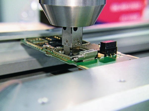
    Micro ball grid array packages (µBGA) rapidly are becoming the package of choice when designing new printed circuit board (PCB) assemblies. These packages
    Veröffentlicht
    06. Juni 2013
    Lesezeit
    1 Minute
    Rubrik
    Applications
    • 1. Higher I/O (input/output) density. As the drive to reduce board size continues, the need for greater I/O density intensifies. The fine-pitch µBGA package offers several times the amount of I/Os per square inch of PCB space than the widely used BGA.
    • 2. Mechanically robust design. The µBGA can be handled without concern for bending and misaligning the leads. This reduces component packaging costs and pre-assembly defect rates of components.
    • 3. More stringent placement tolerances. Standard BGAs typically offer a much larger pitch between terminals, making them more forgiving in terms of placement accuracy. The µBGA and land grid array (LGA) with their smaller ball size and lower pitch require more accurate placement. Typically, a machine with a placement accuracy of 1mil is required. Likewise, the use of lead-free solders presents additional challenges, including decreased occurrences of self-centering during reflow and the inability to rely on the surface tension of the solder self-centering the device as in the past with standard, leaded BGAs.
    • 4. Direct thermal path. In terms of heat dissipation from component to PCB, the LGA’s center ground pad provides a direct path for heat to dissipate into the board. This reduces the thermal resistance of the interconnections, thus minimizing the likelihood of damage to the chip and internal wire bonds.
    • 5. Ease of stencil printing. The LGA makes the stencil printing process a requirement for rework since these components are supplied without solder. An LGA stencil plate must be designed to meet the requirements of the pattern and be fitted to the rework machine.
    • 1. Reflow (for removal)
    • 2. Site preparation
    • 3. Solder paste or flux deposition
    • 4. Placement
    • 5. Reflow

    Mehr aus Applications

    Weitere aktuelle Artikel aus der Rubrik Applications.

    Alle Applications-Artikel
    Expert to highlight new solder paste in Rosemont
    Applications

    Expert to highlight new solder paste in Rosemont

    25. August 2025

    AIM Solder is participating in the upcoming SMTA International 2025 event, which is taking place from October 19–23 at the Donald E. Stephens Convention

    Selective soldering machine take production to a new level
    Applications

    Selective soldering machine take production to a new level

    27. Mai 2025

    Under the motto “Assembling the Future”, Phonotronica Ltd. has been a pioneer in the development and manufacture of electronic modules since 1990.

    ← Zurück zu ApplicationsZur Startseite