Zum Inhalt springen
EPP Europe
  • News
  • Products
  • Applications
  • Technology
  • Semiconductor
  • Inspection
  • Company News
  • Events
EPP Europe
  • Technology
  • Inspection (AOI/AXI)
  • Semiconductor Packaging
  • Company News
  • Products
  • Trade Shows & Events
    EPP Europe Newsletter
    The most important electronics-manufacturing news delivered to your inbox.

    Info

    • Impressum
    • Datenschutz
    • Barrierefreiheit
    • Datenschutzeinstellungen

    Kontakt zur Redaktion

    EPP EuropeKonradin Mediengruppe
    Ernst-Mey-Str. 8, 70771 Leinfelden-Echterdingen

    E-Mail: redaktion@konradin.de
    Folgen Sie uns
    EPP Europe
    © 2026 EPP Europe
    Startseite/Hersteller/Sonoscan

    Sonoscan

    Alle Meldungen, Produkte und Entwicklungen rund um Sonoscan.

    5 Meldungen

    IEEE Rayleigh Award to Dr. Kessler
    News

    IEEE Rayleigh Award to Dr. Kessler

    29. Oktober 2009

    On September 21 in Rome, Italy, Sonoscan president Dr. Lawrence W. Kessler received the prestigious Rayleigh Award presented by the Ultrasonics,

    Sorts out the right echoesFoto: Florian Olivo / Unsplash
    Products

    Sorts out the right echoes

    29. Oktober 2009

    Sonoscan has unveiled some of the details that enable its powerful new software tool to perform acoustic imaging to identify anomalies and defects in
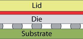
    Providing efficient thermal conduction Tom Adams, Sonoscan Elk Grove Village, IL USA, and Rex Lee, Texas Instruments
    Applications

    Providing efficient thermal conduction Tom Adams, Sonoscan Elk Grove Village, IL USA, and Rex Lee, Texas Instruments

    5. November 2008

    One of the most important elements in electronics systems that require high performance is the thermal interface material (TIM) that bonds the
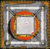
    Patent on virtual rescanning acoustic microscope
    Applications

    Patent on virtual rescanning acoustic microscope

    28. September 2006

    Sonoscan, Inc., the designer and maker of acoustic microscope systems, has been granted a US Patent covering the firm’s Virtual Rescanning Module (VRM).

    Acoustic imaging of bonded wafers
    News

    Acoustic imaging of bonded wafers

    1. Oktober 2002

    Sonoscan's AW2000 systemfor automated inspection of bonded wafer can handle objects up to 200mm in diameter, which is especially useful in imaging after

    Newsletter

    EPP Europe Newsletter

    The most important electronics-manufacturing news delivered to your inbox.

    Jetzt anmelden