
Zum Inhalt springen
EPP Europe
  • News
  • Products
  • Applications
  • Technology
  • Semiconductor
  • Inspection
  • Company News
  • Events
EPP Europe
  • Technology
  • Inspection (AOI/AXI)
  • Semiconductor Packaging
  • Company News
  • Products
  • Trade Shows & Events
    EPP Europe Newsletter
    The most important electronics-manufacturing news delivered to your inbox.

    Info

    • Impressum
    • Datenschutz
    • Barrierefreiheit
    • Datenschutzeinstellungen

    Kontakt zur Redaktion

    EPP EuropeKonradin Mediengruppe
    Ernst-Mey-Str. 8, 70771 Leinfelden-Echterdingen

    E-Mail: redaktion@konradin.de
    Folgen Sie uns
    EPP Europe
    © 2026 EPP Europe
    Startseite/Semiconductor-packaging/Artikel
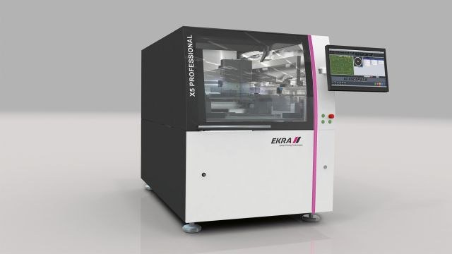
    X5 Professional Optilign and X5 Professional Optilign MultiCarrier
    Bildquelle nicht angegeben
    Semiconductor-packaging

    X5 Professional Optilign and X5 Professional Optilign MultiCarrier

    EKRA Automatisierungssysteme GmbH, a member of the ASYS Group, is located in the high-tech mechanical engineering region Stuttgart. EKRA is a development
    Veröffentlicht
    12. Juli 2022
    Lesezeit
    2 Minuten
    Rubrik
    Semiconductor-packaging

    One focus is on the ongoing miniaturisation of electronics. Ever smaller designs make it possible to penetrate new, previously unexplored areas. Miniaturisation requires new processes and equipment to be able to process such complex components.

    The printing systems X5 Professional Optilign and X5 Professional Optilign MultiCarrier has been designed to achieve highest flexibility, superior throughput, and yields. With its patented Optilign multi substrate alignment we are able to process small, complex, odd shaped designed substrates or the solution for SiP (system in package) modules.

    EKRA X5 Professional Optilign
    EKRA X5 Professional Optilign

    The patented Optilign combines the precision of optical alignment and maximum available print format to gain ideal throughput. As cleaning cycle are print stroke depended, the number of wipes is reduced dramatical as well. As per every wipe an N-Number of substrates been processed before. A clear advantage compared to single substrate processing as know whereas you clean on a very narrow cycle. Depending on substrate size the X5 Professional can manage up to 50 individual pieces within one workholder.

    Another way to use Optilign is Optlign Multi Carrier. Multi Carrier has been developed to boost throughput once more when manufacturing is limited to a certain carrier / workholder size. The X5Professional Optilign Multicarrier is able to collect as many substrates as can ideally be handled with the maximum print area of the system. Means customer do not need to invest into newer enlarged carriers and adapt other production equipment because of getting more printed substrates. X5Professional Multi Carrier collects, prints and delivers afterwards carrier by carrier back to the downstream.
    This innovative solution increase throughput by almost 3 times!

    Mehr aus Semiconductor-packaging

    Weitere aktuelle Artikel aus der Rubrik Semiconductor-packaging.

    Alle Semiconductor-packaging-Artikel
    Nanoscribe Expands Photoresin Portfolio for Micro-Optics Fabrication via Two-Photon PolymerizationFoto: Brecht Corbeel / Unsplash
    Semiconductor-packaging

    Nanoscribe Expands Photoresin Portfolio for Micro-Optics Fabrication via Two-Photon Polymerization

    11. November 2026

    Nanoscribe has detailed its range of photoresins engineered for Two-Photon Polymerization (2PP) and Two-Photon Grayscale Lithography (2GL), targeting high-precision micro-optics manufacturing on silicon, glass, and…

    Canon Launches FPA-6400ES6a KrF Lithography System with 400 Wafers-per-Hour ThroughputFoto: Canon Europe (semicon)
    Semiconductor-packaging

    Canon Launches FPA-6400ES6a KrF Lithography System with 400 Wafers-per-Hour Throughput

    10. November 2026

    Canon has announced the FPA-6400ES6a KrF scanner for semiconductor lithography, combining a throughput of 400 wafers per hour with industry-leading overlay accuracy of 4.0 nm and the ability to handle wafer warpage of…

    Fabmatics absorbs SCI business activities under unified brandFoto: Ludovico Ceroseis / Unsplash
    Semiconductor-packaging

    Fabmatics absorbs SCI business activities under unified brand

    6. November 2026

    Fabmatics has integrated the business activities of SCI under the Fabmatics brand, consolidating the acquired expertise within its semiconductor automation portfolio.

    Entegris and Kioxia Expand Partnership on Materials Innovation for Next-Gen 3D Flash MemoryFoto: Louis Reed / Unsplash
    Semiconductor-packaging

    Entegris and Kioxia Expand Partnership on Materials Innovation for Next-Gen 3D Flash Memory

    6. November 2026

    Entegris and Kioxia are deepening their strategic partnership to co-develop materials and process technologies for future BiCS FLASH 3D NAND architectures, using AI, digital-twin modelling and experimental validation at…

    ← Zurück zu Semiconductor-packagingZur Startseite


