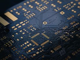

The progressive miniaturisation of electronic assemblies has fundamentally changed the inspection challenge in SMT manufacturing. Ball grid arrays, quad-flat no-leads packages, chip-scale packages and embedded components all share one critical characteristic: their solder joints are hidden beneath the component body and therefore inaccessible to optical inspection methods. Automated optical inspection, however sophisticated, cannot see through silicon or moulding compound. X-ray inspection fills precisely this gap by exploiting the differential absorption of ionising radiation in materials of different atomic mass and density.
X-ray systems have been used in electronics production since the late 1980s, initially as off-line laboratory tools for failure analysis. The transition to in-line, real-time capable systems suitable for production feedback took several decades of development in detector technology, image processing and tube design. Today, both 2D and 3D X-ray platforms are routinely integrated into high-volume SMT lines, and their role extends well beyond simple pass/fail decisions to quantitative void analysis, joint geometry measurement and process optimisation.
Physical Principles: How X-Ray Inspection Works
X-ray inspection is based on the attenuation of electromagnetic radiation as it passes through matter. When a focused X-ray beam traverses an assembly, different materials absorb photons to different degrees depending on their atomic number, density and thickness. Lead-free solder alloys — predominantly tin-silver-copper compositions — attenuate X-rays significantly more than the surrounding printed circuit board substrate, copper conductors or component housings. This differential attenuation produces contrast in the transmitted image, making solder joints visible against the background of the board.
Gas voids within solder joints appear as darker regions in a transmission image because the void contains no attenuating material. Bridging between adjacent joints manifests as a locally brighter, continuous region of elevated absorption. Missing balls in a BGA array become apparent as the absence of the characteristic circular absorption pattern. These phenomena are consistent and physically well-defined, which is why X-ray inspection can be evaluated algorithmically with high repeatability.
2D Transmission Versus 3D Computed Tomography: System Architectures Compared
The most common distinction in production X-ray systems is between 2D transmission imaging and three-dimensional computed tomography, often referred to as AXI (automated X-ray inspection) in its production-oriented form. In a 2D transmission system, the X-ray source and a flat-panel detector are positioned on opposite sides of the board. The resulting image is a projection — a superposition of all material layers the beam traverses. This superposition creates ambiguity when top-side and bottom-side components overlap, and it limits the ability to isolate individual solder joint layers on double-sided assemblies.
3D AXI systems acquire multiple projection images at different angles and reconstruct volumetric cross-sections using algorithms derived from medical CT technology. This approach allows individual solder joint layers to be examined in isolation, independent of overlapping features on the opposing board side. Laminographic reconstruction — a computationally efficient approximation of full CT particularly suited to flat objects such as PCBs — is the dominant method in production AXI equipment. Full computed tomography with 360-degree rotation is generally reserved for laboratory analysis and high-value component verification rather than in-line throughput-driven inspection.
The trade-off between 2D and 3D systems involves throughput, capital cost and inspection depth. 2D systems are faster and less expensive; they are well suited to single-sided assemblies or boards where component overlap is not a systematic problem. 3D AXI justifies its higher cost on complex double-sided assemblies, densely populated boards and applications where quantitative void measurement in BGA joints is a process requirement.
Key Inspection Applications and Measurable Defect Classes
The primary production application of X-ray inspection is BGA and CSP joint quality assessment. Industry standards such as IPC-7095 define void acceptance criteria for BGA solder joints; depending on the application class and joint diameter, void areas exceeding a defined percentage of the total joint cross-section are considered non-conforming. X-ray systems measure void area or volume and compare it against these thresholds automatically. This capability is particularly important in automotive, aerospace and high-reliability industrial electronics, where thermal cycling and mechanical stress make voiding a genuine reliability risk.
Beyond BGA inspection, X-ray is applied to through-hole solder fill verification — checking that solder has penetrated to the required depth in plated through-holes without excessive exposure on the component side. Press-fit connector inspection, verification of solder paste volume in stencil printing (where X-ray complements SPI in specific applications) and analysis of solder joint geometry for QFN and LGA packages are further established use cases. Counterfeit component detection, particularly identifying remarked or reballed BGAs, is an emerging application area in which X-ray evidence of internal construction is compared against authentic reference images.
Tube Technology, Magnification and Image Quality Parameters
The X-ray source — the tube — determines resolution, contrast and applicable voltage range. Sealed microfocus tubes generate a small focal spot, typically in the range of a few micrometres, enabling high geometric magnification without significant loss of sharpness. Open tube systems, in which the target can be replaced, offer the smallest achievable focal spots and highest resolution but require more complex maintenance. The operating voltage, commonly between 80 kV and 160 kV for PCB inspection, governs penetration depth and contrast: lower voltages provide better contrast between solder and board materials; higher voltages are necessary to penetrate thick copper planes or metal housings.
Detector technology has advanced substantially with the adoption of flat-panel detectors based on amorphous silicon or caesium iodide scintillators, replacing older image-intensifier tube designs. Modern flat-panel detectors offer improved dynamic range, reduced geometric distortion and faster frame rates, all of which contribute to both image quality and system throughput. Signal-to-noise ratio at the detector level directly influences the minimum detectable void size and the repeatability of quantitative measurements.
Integration into the SMT Line and Process Feedback
In production environments, AXI systems are typically positioned after reflow soldering and may operate in parallel with or downstream of AOI stations. The two inspection modalities are complementary rather than redundant: AOI covers component presence, polarity, coplanarity and visible solder joint quality; AXI addresses hidden joint integrity. A combined inspection strategy using both methods achieves higher defect coverage than either alone, and the classification of defects by type informs which upstream process step requires corrective action.
Closed-loop feedback from AXI to the reflow oven — or to the stencil printer via SPI data correlation — is a recognised practice in advanced manufacturing environments operating under statistical process control. Systematic void patterns across a BGA array, for instance, can indicate a thermal profile issue or a solder paste outgassing problem rather than a random defect. Traceability systems that link X-ray inspection results to individual boards, production batches and process parameters make this kind of root-cause analysis tractable.
Application Limits and Practical Considerations
X-ray inspection is not a universal solution for all defect classes. It does not replace functional test or in-circuit test for detecting electrical opens that result from lifted bonds, cracked vias or ESD-induced component damage not visible in joint geometry. Component-level defects such as incorrect component value or parametric drift are outside its scope. Radiation safety requirements impose infrastructure costs and regulatory obligations that must be factored into facility planning. Throughput constraints in 3D AXI — inspection times per board can range from under a minute for simple 2D scans to several minutes for high-resolution 3D reconstructions — require careful line balancing in high-volume operations.
As component packages continue to evolve — with embedded dies, multi-chip modules and heterogeneous integration introducing new joint geometries and material stacks — X-ray inspection methodology must adapt accordingly. The development of higher-resolution detector arrays, artificial-intelligence-assisted image evaluation and standardised void measurement protocols reflects an inspection discipline that remains central to the quality infrastructure of advanced electronics manufacturing, not as a final gatekeeper, but as a continuous source of process intelligence.