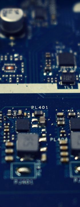
Despite the broad advance of surface mount technology, wave soldering continues to occupy an indispensable role in electronics production. Many assemblies combine SMT components on the top side with through-hole connectors, relays or power components on the underside — a configuration commonly referred to as mixed-technology or hybrid assembly. In these cases, wave soldering provides a cost-efficient and highly parallel method for forming reliable solder joints on dozens or hundreds of through-hole pins in a single pass. Understanding how the process works, which parameters govern joint quality and what machine architectures are available is foundational knowledge for process engineers and quality managers alike.
Wave soldering is a mass-soldering technique in which a printed circuit board (PCB) is transported over one or more standing waves of molten solder. The wave contacts the underside of the board, fills plated-through holes by capillary action and wets component leads to form intermetallic joints. The process is sequential: fluxing, preheating and soldering occur in defined zones within a single inline machine, typically followed by cooling. Each stage influences the metallurgical and mechanical quality of the finished joint.
Flux Application: The Chemical Foundation of Wettability
Flux is applied before the board enters the solder wave. Its primary function is to remove oxide layers from both the PCB pad surfaces and the component leads, thereby enabling intimate metal-to-metal contact and promoting wetting by the molten solder. Three principal flux application methods are used in industrial machines: foam fluxing, spray fluxing and wave fluxing. Spray fluxing — applying flux as a fine aerosol via ultrasonic or pressure nozzles — has become the dominant method in modern equipment because it enables precise flux quantity control, supports low-solids and no-clean flux chemistries, and reduces the risk of flux contamination in protected board areas.
Flux chemistry is classified according to IPC J-STD-004 by activator type and solids content. Rosin-based (RO), resin-based (RE), organic acid (OR) and synthetic activated (SA) fluxes each carry specific activity levels — low (L), medium (M) or high (H) — and halide content designations. No-clean fluxes leave residues that are designed to be electrochemically benign and need not be removed; water-soluble fluxes deliver high activity but require subsequent aqueous cleaning. The choice of flux must be compatible with the solder alloy, board finish, component types and any downstream requirements such as conformal coating.
Preheating: Thermal Preparation and Its Influence on Joint Formation
After fluxing, the board passes through a preheat zone whose purpose is threefold: activating the flux (initiating oxide removal), evaporating flux solvents to prevent solder spattering at the wave, and raising the board and component temperature to reduce thermal shock and minimise cold solder joint formation. Preheat zones employ infrared emitters, forced convection or a combination of both. Convection preheating offers more uniform thermal distribution across complex, thermally disparate assemblies.
Target preheat temperatures at the board underside typically range from 90 °C to 130 °C for no-clean flux systems, though the exact profile must be validated for each assembly. Insufficient preheat results in incomplete flux activation and residual solvent, which causes solder balls and voids. Excessive preheat degrades flux activity prematurely and can thermally stress sensitive components. Process engineers use thermocouple profiling or thermal imaging to map the actual temperature distribution across the board before finalising preheat settings.
The Solder Wave: Hydrodynamics, Alloy Behaviour and Machine Architectures
The solder wave itself is generated by an electromagnetic or mechanical pump that circulates molten solder from a reservoir through a nozzle, creating a stable, upwelling flow against which the board is transported. Modern machines typically employ a dual-wave configuration: a first, turbulent chip wave (also called a lambda or Ω wave) followed by a second, smooth laminar wave. The chip wave ensures penetration of solder beneath closely spaced SMT components soldered on the underside (glued in place prior to wave soldering), while the laminar wave provides the controlled, drainage-friendly surface that produces well-formed fillets and removes bridging.
Solder alloy composition critically determines wave behaviour, joint microstructure and reliability. Traditional tin-lead alloys (Sn63Pb37, eutectic at 183 °C) have been largely replaced by lead-free alloys under RoHS regulation. The most widely adopted lead-free wave alloy is SAC305 (Sn96.5Ag3.0Cu0.5), with a liquidus temperature of approximately 219 °C. This higher process temperature imposes greater thermal load on boards and components and demands careful management of dross formation, as lead-free alloys are more prone to oxidation. Alloy additives such as nickel, germanium or bismuth are used by some manufacturers to reduce dross, improve fluidity and extend pot life.
Key machine parameters include conveyor speed, wave contact length and contact time, wave height, solder temperature (typically 255–265 °C for SAC305) and conveyor inclination angle. Contact time — the duration the board underside is in contact with the solder wave — is inversely proportional to conveyor speed and directly related to wave geometry. Typical contact times lie between 2 and 4 seconds per wave. Nitrogen inerting of the solder pot and wave zone significantly reduces dross formation and improves wettability, enabling lower process temperatures and better joint appearance, particularly with lead-free alloys.
Tooling, Pallets and the Challenge of Mixed-Technology Boards
When SMT components are present on the underside of a mixed-technology board, solder thieves, masking tapes or dedicated wave-solder pallets are required to protect those components and their solder joints from the wave. Pallets — typically manufactured from glass-fibre-reinforced PTFE, aluminium or titanium-filled composites — expose only the through-hole areas to the solder wave while shielding SMT regions. Pallet design directly influences shadowing defects, solder skips and bridging, and must account for board warpage, thermal expansion and adequate flux access to all joints.
Component lead protrusion length on the underside of the board is another critical variable. IPC-A-610 specifies acceptable protrusion ranges, as insufficient protrusion limits hole fill, while excessive protrusion causes bridging or interference with the wave geometry. Board design, component selection and assembly sequencing must therefore be coordinated from the earliest stages of product development to ensure wave-solder compatibility.
Defect Mechanisms, Process Control and Quality Verification
Common wave-solder defects include bridging (solder shorts between adjacent leads), insufficient hole fill, icicles, solder balls, pin holes and disturbed joints. Bridging typically originates from excessive solder volume, incorrect conveyor angle, insufficient wave drainage or contaminated flux. Insufficient hole fill results from inadequate preheat, poor flux activation, excessive conveyor speed or board design issues such as large thermal masses at ground planes. Each defect has identifiable root causes traceable to specific process parameters, which is why systematic design-of-experiment (DOE) approaches and statistical process control (SPC) are integral to mature wave-solder processes.
Automated optical inspection (AOI) and X-ray inspection (AXI) are the primary verification tools applied after wave soldering. AOI detects surface-visible defects such as bridging, missing joints and gross solder volume deviations. AXI is essential for evaluating through-hole fill levels and detecting voids inside barrel joints that are not optically accessible. IPC-A-610 Class 2 and Class 3 acceptance criteria define minimum hole fill requirements (75 % and 100 % respectively from the solder source side) and serve as the industry-standard quality benchmark.
Process Optimisation and Outlook
Wave soldering process optimisation is an iterative discipline combining thermal profiling, alloy monitoring, flux activity measurement, SPC on defect data and regular machine maintenance — including solder pot analysis for copper, silver and contaminant accumulation. Inert-atmosphere machines and advanced pump designs continue to push the boundaries of joint quality and yield, particularly for high-density, fine-pitch through-hole applications. While selective soldering is increasingly chosen for assemblies with isolated through-hole components on otherwise fully SMT boards, wave soldering retains clear economic and throughput advantages for high-volume production with significant through-hole content. Mastery of its process fundamentals remains a core competence in professional electronics manufacturing.