
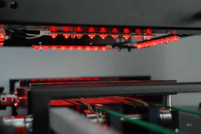
Using lasers for marking the backside of silicon wafers is getting more and more attractive for products with packaging that leaves the backside of the silicon chip exposed. Chip scale packaging, direct chip attach and flip chip technology are major types to mention in this context.
In both applications – SMT and Semiconductor Backend – no need for consumables and the speed of processing lead to the low COO of the laser marking process.
In addition a contactless operation helps to avoid ESD.

Common available laser technologies start from the long wavelength IR low power CO2 lasers at 10.600 nm through NIR DPSS laser or fiber lasers at 1064 nm to DPSS lasers with SHG at 532 nm or THG at 355 nm.
Converting DPSS lasers from the fundamental NIR wavelength to VIS green or UV is often called frequency doubling or tripling.
The beam steering in laser systems is common for all useful wavelengths. So called Galvo Scanners use galvanometric beam deflection by mirrors to position the laser beam very fast and precise. Appropriate f-theta lenses and beam expanders allow for the right laser spot size and working area in XY commonly called scan field.

The type of laser beam sources used for marking are process specific. Lasers in IR show no absorption in silicon and are useless for Semiconductor Packing therefore as almost 100 % of the laser radiation is being reflected.
Absorption of NIR is low in silicon at room temperature and increases with temperature. This effect allows to use specific fiber lasers for laser marking silicon. Fiber lasers are well established in electronic industries due to their ease of integration and low maintenance and come at an attractive price. Especially MOPA fiber lasers with their wide range of laser parameters including pulse length can be used effectively for laser marking applications.
Using 532 nm green lasers for silicon marking benefits from three arguments. Absorption is higher and the penetration depth in silicon is limited to the surface only thus limiting the risk for active structures on the front side when marking the backside of the wafer. In addition the shorter wavelength allows for smaller spot sizes.
UV lasers are even excelling green lasers in terms of absorption and penetration depth. Nevertheless they are used for dedicated applications only due to their high COO.
Using 532 nm green lasers for wafer backside marking we distinct between different processes. The process is determined by the energy density or fluence applied to the material:
Engraving marking
Black marking with character height 0,2 mm. The engraving depth was measured as 8 to 14 µm depth. We achieved a marking speed of 335 char/sec.

Annealing marking
White marking with character height of 0.3 mm. The marking depth was measured below 5 µm. We achieved a marking speed of 385 char/sec.

Invisible marking
When decreasing the energy level below the ablation threshold of the material we found a marking which is hardly seen by the human eye. The marking effect can be characterized as surface alteration of the silicon.
Invisible marking with a character height of 0,2 mm. The marking depth was measured again below 5 µm. We achieved a marking speed of 216 char/sec.

Epoxy Overmold
To mark on epoxy overmold we found NIR MOPA fiber lasers as the most useful technology.
An example of application was to apply a Data Matrix Code (DMC) with a size of 3 mm x 3 mm with 18 numeric characters (16×16 Code) on an ASICS epoxy package housing. The marking showed a good white on black contrast.
Marking time was 0,4 sec per Code. The penetration depth was around 20 µm only.

Glossary:
COO – Cost of ownership
DMC – Data Matrix Code
DPSS – Diode pumped solid state
ESD – Electro static discharge
IR – Infrared
MOPA – Modulator power amplifier
NIR – Near infrared
SHG – Second harmonic generators
THG – Third harmonic generator
UV – Ultra violet
VIS – Visible



